
This tutorial will show you how to create simple single layer PCB's at home without any hassle :hap2:
[BREAK=Introduction]
Being an IT guy it is sometimes difficult to get involved into projects that involve hardware and circuits. Most people buy standard development boards, use bread boards for the circuits or spend hours soldering it. Being such a guy I was in a fix as the development boards did not solve my purpose, wires on the bread board kept coming out and I am very bad at soldering (my circuit was pretty big too). One of my electronics friends suggested me this awesome method of creating custom printed circuit boards (PCB’s) at home without much hassle. So here goes my first tutorial.
Prerequisites
1. Ability to make circuits on bread board.
2. Little experience with soldering.
3. A bit of drilling experience will help.
Components/Software’s required (Refer to the respective section for pictures)
1. PCB designing software (here we will use Diptrace).
2. Your circuit (of course).
3. Glossy paper (ones used for printing photos).
4. Copper board.
5. Drill with .5mm bit.
6. Ferric Chloride (FeCl3) liquid.
7. Normal iron that is used for ironing clothes.
8. Nail polish remover/thinner/turpentine oil.
9. Tape
[BREAK=Downloading and installing Diptrace]
Download and install the Diptrace freeware version with libraries from http://www.diptrace.com/downloads/dipfree_en.exe
We will not be dwelling much into the software as this tutorial is about how to create the PCB from the design. You can refer to Diptrace help and read this tutorial on how to create the design. http://www.diptrace.com/books/tutorial.pdf
The standard libraries will take into account almost all the components you will ever require. Do the following steps. Refer the above tutorial on how to do the same.
1. Open the schematic.
2. Place your components and do the necessary connections.
3. Press Ctrl+B to open the PCB layout.
Once the layout is in front of you do the following
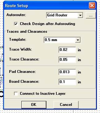
1. Select Route-> Route Setup
2. From the template select .5mm (you can also select larger if your circuit is simple but selecting anything lesser might not give proper results).
3. Change other values corresponding to the following and select OK.
View attachment 4451
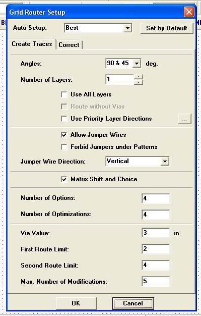
4. Select Route->Autorouter Setup and select the following (you can increase the “number of options†and “number of optimizations†for better results but it will take more time while routing). Select OK.
View attachment 4453
5. Click on Route->Run Autorouter or press F9.
6. Wait for the auto routing to complete.
If there are no errors then you should have a design in front of you. If you are dissatisfied with the results then simply rotate the components and do the process again till you get good results.
For larger circuits it may take some tries to get the job done properly. If the router is not able to create a perfect PCB then you can create some pads and connect them later with wires but make sure that there are not many wires. Again designing would be a different tutorial itself hence I will not get into more detail. Refer to the help and the guide of Diptrace to learn how to create perfect PCB’s.
Note: Diptrace is just one of the software. There are many more such as OrCAD, Altium etc. You can use any one to design your PCB.
Now towards part 2
[BREAK=Printing]
The print will be taken on a glossy paper from a laser printer. We choose laser printer because the toner ink can be easily transferred to the copper board. Since I do not have a laser printer, I had to get one from a local cybercafé (I had to ask him to install the software). You can also try offices or school/colleges.
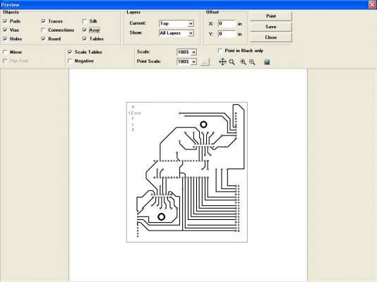
From Diptrace select File->Preview and select the following
Make sure that you select print scale as 100% otherwise the size of the components will not be equal to the one on the print.
View attachment 4452
Take a test print on a normal paper (for this even an inkjet will do) and verify the size on ICs’ on the print is same as that of the actual IC by simply placing the IC on the print.
Now insert the glossy paper such that the print comes on the glossy side and select print from a laser printer. Once the print out has been taken it should look like this.
View attachment 4467
Fit the IC’s and verify that the size of the components in the print is same as the actual size.
Note: You might have noticed the save option that saves the PCB as a bmp or jpg. You can also save it and then take the print of the image, however I was not able to bring it to scale (i.e. size of the IC’s were not same on the print). If saving works for you then you will not have to install the software on the PC connected to the laser printer.
Now that printing is done, we move to part 3
[BREAK=Transferring the image on to the copper board]

1. Switch ON the iron and wait for it to heat.
2. Put on some gloves if possible so that you do not burn your hands later on.
3. Cut the glossy paper to the size of the copper board.
4. Dip the glossy paper once for 2-3 seconds in water, quickly take it out (dipping in water optional) and put the printed face down on the copper board.
5. Press the paper with your hand to remove any air bubbles between the copper board and the paper.
6. Tape the four corners of the paper to the copper board.
7. Place the copper board on a flat surface.
View attachment 4470
8. Take the hot iron and press it on the paper. Keep ironing for about 4-5 minutes. If the paper gets dry before you start ironing then sprinkle a little water on it and start ironing.
9. CAUTION: DO NOT TOUCH THE COPPER BOARD AS IT IS GOING TO BE VERY HOT.
10. Wait 5-10 minutes for the copper to cool down.
11. Dip the copper board with the paper taped to it in a bucket of water.
12. Gently rub it and remove all of the paper.
13. You will notice that all the tracks and pads have been transferred to the copper board.
Note: If you want to add anything else like a logo or your name, simply use a black permanent marker to write on the copper board. Write over and over again so that the ink of the marker becomes permanent.
You can also use the marker to write on top of the tracks that you think have not come properly
Now for part 4
[BREAK=Etching]
View attachment 4464
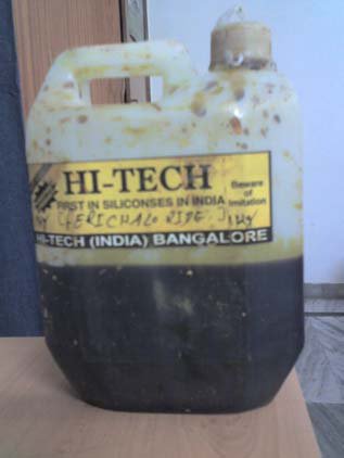
1. Take the Ferric Chloride (FeCl3) liquid and pour it in a container big enough to hold the copper board completely (use some Tiffin box or so). The container should be made of only plastic or glass. Do not use metal container because Ferric Chloride will react with it.
View attachment 4473
2. Dip the board completely in the ferric chloride liquid and leave it for 45 minutes.
3. Take the board out and wash it with water, you should only see a plastic base with the toner ink on top like this. If there is any copper remaining then immerse the board in FeCl3 again and leave for another 10 mins.
4. Once you have the board with only toner ink then take some thinner/nail polish remover/turpentine oil, pour it in cotton and rub the board with it to remove the ink and get only copper tracks and pads.
View attachment 4469
Note: If you find FeCl3 powder then also the procedure will work by mixing the powder with water in a specific proportion.
You can check the continuity of tracks using a multimeter. If there are some tracks that are not continuous or not satisfactory, then you can simply put a drop of solder over that point.
Now for the last part
[BREAK=Drilling and Soldering]
View attachment 4463
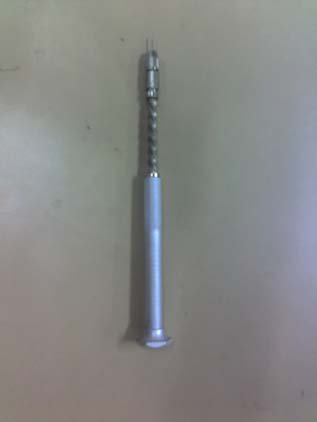
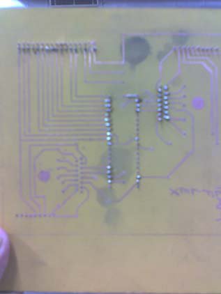
1. Take a drill with bit of .5mm or so (make sure that it is no thicker than the pads) and drill all the pads of the PCB.
2. Place your components or holders.
3. Solder the bases of the holders/components to the tracks and you are done.


Note: Be careful while drilling, even though the bit is quite strong it may break upon constant usage.
[BREAK=Pricelist]
Pricelist
I got all my components from Lajpat Rai Market in Delhi. Other people will easily find them in the local electrical market. Ferric Chloride can be obtained from any chemical store. Here is the approximate price list.
1. Copper Board : Rs 50 / board
2. Glossy paper : Rs 10/paper
3. FeCl3 liquid : Rs 165/liter (it may be cheaper)
4. Manual Drill with bit : <Rs 50
5. Thinner/Nail polish remover/Turpentine oil : Rs 12/Rs 35/Rs 40 respectively
6. Printing charges: Re 1/print
[BREAK=Concluding Remarks]
First of all I would like to thank my friend for explaining this procedure to me. I am not a PCB wiz and there may be many methods better than this, I just found this one the easiest. If there are any such tutorials on the internet I have not seen them and thus have not added any references. Any other comments, suggestions, criticisms or additions will be highly appreciated.
Good luck with your PCB.
[BREAK=Introduction]
Being an IT guy it is sometimes difficult to get involved into projects that involve hardware and circuits. Most people buy standard development boards, use bread boards for the circuits or spend hours soldering it. Being such a guy I was in a fix as the development boards did not solve my purpose, wires on the bread board kept coming out and I am very bad at soldering (my circuit was pretty big too). One of my electronics friends suggested me this awesome method of creating custom printed circuit boards (PCB’s) at home without much hassle. So here goes my first tutorial.
Prerequisites
1. Ability to make circuits on bread board.
2. Little experience with soldering.
3. A bit of drilling experience will help.
Components/Software’s required (Refer to the respective section for pictures)
1. PCB designing software (here we will use Diptrace).
2. Your circuit (of course).
3. Glossy paper (ones used for printing photos).
4. Copper board.
5. Drill with .5mm bit.
6. Ferric Chloride (FeCl3) liquid.
7. Normal iron that is used for ironing clothes.
8. Nail polish remover/thinner/turpentine oil.
9. Tape
[BREAK=Downloading and installing Diptrace]
Download and install the Diptrace freeware version with libraries from http://www.diptrace.com/downloads/dipfree_en.exe
We will not be dwelling much into the software as this tutorial is about how to create the PCB from the design. You can refer to Diptrace help and read this tutorial on how to create the design. http://www.diptrace.com/books/tutorial.pdf
The standard libraries will take into account almost all the components you will ever require. Do the following steps. Refer the above tutorial on how to do the same.
1. Open the schematic.
2. Place your components and do the necessary connections.
3. Press Ctrl+B to open the PCB layout.
Once the layout is in front of you do the following
1. Select Route-> Route Setup
2. From the template select .5mm (you can also select larger if your circuit is simple but selecting anything lesser might not give proper results).
3. Change other values corresponding to the following and select OK.
View attachment 4451
4. Select Route->Autorouter Setup and select the following (you can increase the “number of options†and “number of optimizations†for better results but it will take more time while routing). Select OK.
View attachment 4453
5. Click on Route->Run Autorouter or press F9.
6. Wait for the auto routing to complete.
If there are no errors then you should have a design in front of you. If you are dissatisfied with the results then simply rotate the components and do the process again till you get good results.
For larger circuits it may take some tries to get the job done properly. If the router is not able to create a perfect PCB then you can create some pads and connect them later with wires but make sure that there are not many wires. Again designing would be a different tutorial itself hence I will not get into more detail. Refer to the help and the guide of Diptrace to learn how to create perfect PCB’s.
Note: Diptrace is just one of the software. There are many more such as OrCAD, Altium etc. You can use any one to design your PCB.
Now towards part 2
[BREAK=Printing]
The print will be taken on a glossy paper from a laser printer. We choose laser printer because the toner ink can be easily transferred to the copper board. Since I do not have a laser printer, I had to get one from a local cybercafé (I had to ask him to install the software). You can also try offices or school/colleges.
From Diptrace select File->Preview and select the following
Make sure that you select print scale as 100% otherwise the size of the components will not be equal to the one on the print.
View attachment 4452
Take a test print on a normal paper (for this even an inkjet will do) and verify the size on ICs’ on the print is same as that of the actual IC by simply placing the IC on the print.
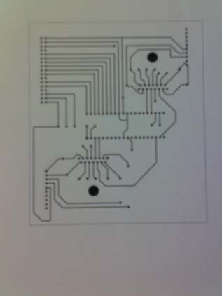
Now insert the glossy paper such that the print comes on the glossy side and select print from a laser printer. Once the print out has been taken it should look like this.
View attachment 4467
Fit the IC’s and verify that the size of the components in the print is same as the actual size.
Note: You might have noticed the save option that saves the PCB as a bmp or jpg. You can also save it and then take the print of the image, however I was not able to bring it to scale (i.e. size of the IC’s were not same on the print). If saving works for you then you will not have to install the software on the PC connected to the laser printer.
Now that printing is done, we move to part 3
[BREAK=Transferring the image on to the copper board]
1. Switch ON the iron and wait for it to heat.
2. Put on some gloves if possible so that you do not burn your hands later on.
3. Cut the glossy paper to the size of the copper board.
4. Dip the glossy paper once for 2-3 seconds in water, quickly take it out (dipping in water optional) and put the printed face down on the copper board.
5. Press the paper with your hand to remove any air bubbles between the copper board and the paper.
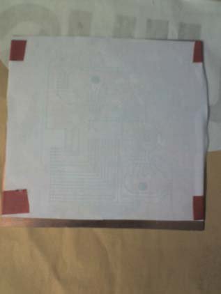
6. Tape the four corners of the paper to the copper board.
7. Place the copper board on a flat surface.
View attachment 4470
8. Take the hot iron and press it on the paper. Keep ironing for about 4-5 minutes. If the paper gets dry before you start ironing then sprinkle a little water on it and start ironing.
9. CAUTION: DO NOT TOUCH THE COPPER BOARD AS IT IS GOING TO BE VERY HOT.
10. Wait 5-10 minutes for the copper to cool down.
11. Dip the copper board with the paper taped to it in a bucket of water.
12. Gently rub it and remove all of the paper.
13. You will notice that all the tracks and pads have been transferred to the copper board.
Note: If you want to add anything else like a logo or your name, simply use a black permanent marker to write on the copper board. Write over and over again so that the ink of the marker becomes permanent.
You can also use the marker to write on top of the tracks that you think have not come properly
Now for part 4
[BREAK=Etching]
View attachment 4464
1. Take the Ferric Chloride (FeCl3) liquid and pour it in a container big enough to hold the copper board completely (use some Tiffin box or so). The container should be made of only plastic or glass. Do not use metal container because Ferric Chloride will react with it.
View attachment 4473
2. Dip the board completely in the ferric chloride liquid and leave it for 45 minutes.
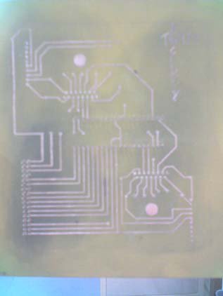
3. Take the board out and wash it with water, you should only see a plastic base with the toner ink on top like this. If there is any copper remaining then immerse the board in FeCl3 again and leave for another 10 mins.
4. Once you have the board with only toner ink then take some thinner/nail polish remover/turpentine oil, pour it in cotton and rub the board with it to remove the ink and get only copper tracks and pads.
View attachment 4469
Note: If you find FeCl3 powder then also the procedure will work by mixing the powder with water in a specific proportion.
You can check the continuity of tracks using a multimeter. If there are some tracks that are not continuous or not satisfactory, then you can simply put a drop of solder over that point.
Now for the last part
[BREAK=Drilling and Soldering]
View attachment 4463
1. Take a drill with bit of .5mm or so (make sure that it is no thicker than the pads) and drill all the pads of the PCB.
2. Place your components or holders.
3. Solder the bases of the holders/components to the tracks and you are done.
Note: Be careful while drilling, even though the bit is quite strong it may break upon constant usage.
[BREAK=Pricelist]
Pricelist
I got all my components from Lajpat Rai Market in Delhi. Other people will easily find them in the local electrical market. Ferric Chloride can be obtained from any chemical store. Here is the approximate price list.
1. Copper Board : Rs 50 / board
2. Glossy paper : Rs 10/paper
3. FeCl3 liquid : Rs 165/liter (it may be cheaper)
4. Manual Drill with bit : <Rs 50
5. Thinner/Nail polish remover/Turpentine oil : Rs 12/Rs 35/Rs 40 respectively
6. Printing charges: Re 1/print
[BREAK=Concluding Remarks]
First of all I would like to thank my friend for explaining this procedure to me. I am not a PCB wiz and there may be many methods better than this, I just found this one the easiest. If there are any such tutorials on the internet I have not seen them and thus have not added any references. Any other comments, suggestions, criticisms or additions will be highly appreciated.
Good luck with your PCB.
Attachments
-
 route setup.JPG60 KB · Views: 196
 -
 print.JPG66.3 KB · Views: 194
 -
 autorouter.JPG71.7 KB · Views: 167
 -
 drill.jpg26.9 KB · Views: 175
 -
 fecl.jpg40.5 KB · Views: 161
 -
 glossyprnt.jpg31.5 KB · Views: 170
 -
 pcb.jpg33.1 KB · Views: 197
 -
 wettaped.jpg30.2 KB · Views: 151
 -
 solder.jpg33.2 KB · Views: 165
 -
 container.jpg29.3 KB · Views: 180
