
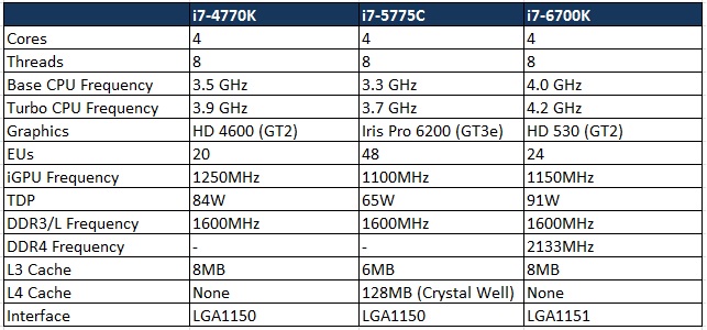
Adapting to Moore’s Law isn’t easy. Intel has been officially on their ‘tick-tock’ program since 2007 with a Tick being the advancement for manufacturing technology in accordance with Moore’s Law, while a Tock a new microarchitecture using the previous ‘tick’ cycle. Their release cadence in between two ‘Tick’s has varied between 18-24 months, gradually shrinking the manufacturing lithographical process to 22nm and increasing the number of transistors in a chip/die. But with the release of Sandy Bridge, Intel produced the last significant performance gap between two tick generations, something that hasn’t been replicated since. Sandy Bridge(and Ivy Bridge) when compared to Haswell and Devil’s Canyon performed admirably and proved to be within 90% performance range, something that deterred many users not to switch. Intel’s per core performance was increasing roughly around 5% per tick cycle. Instead we saw a gradual focus shift from Intel to generally correct their problems with thermals and power consumption – a critical flaw for Ivy Bridge generation was how hot the chips ran. During the last few tick-tocks the definition of overclocking also changed significantly; my core i7-2600K could easily do 5GHz+ with an AIO CPU cooler, but talk to anybody using Ivy Bridge and later and they would tell you that reaching 4.5GHz on decent cooling is equivalent of you having a golden chip. Exotic cooling methods pushed the Haswell chips beyond 6GHz, but it was definitely hard to get a sample that would bench near 5GHz with AIO/custom liquid cooling.
 The Skylake launch has been interesting from many aspects. Around last year Intel announced that they ran into yield issues with 14nm FINFET process. That troubled them for quite some time, and as a direct result desktop Broadwell parts were limited at launched. Bearing the impossible task to replicate Moore’s Law in their cycle, Intel had to sacrifice either one: and with Skylake it seems that they are going to stretch the latter. Kaby Lake, now delayed to second half of 2017 will be based on the same 14nm process – meaning that for the first time we will be seeing a tick-tock-tock from Intel, and their release cycle will be stretched to 36months+ for the shift to 10nm to arrive. This change in strategy can be beneficial for Intel, since it gives them ample time to perfect the 14nm process, something we have seen NVidia do with the Maxwell GPUs (the GPU manufacturing process seems to be stuck in 28nm since forever). Broadwell introduced some new instruction set extensions (Intel ADX/RDSEED/PREFETCHW/SMAP) into an already perfected 22nm Haswell and gave it a die shrink. Skylake is released barely a year after Broadwell to advance the cause for Intel – can it become its shining knight?
What’s new with Skylake?
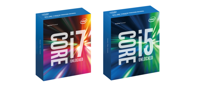
Before we delve into the technical details, let’s first look at the most immediate change: retail packaging. The desktop Skylake chips will be using a colourful box, a stark departure from the monotonous blue/black boxes that Intel has been offering. As of now we get to see two box-shots, though it is safe to assume that with the release of more processors, we will see a variety of packaging for Skylake.
 With Skylake Intel is also releasing a new chipset, dubbed Z170. While Broadwell worked on the same LGA1150 socket as Haswell/Devil’s Canyon, this changes with Skylake. The socket is now LGA1151 (though the CPU cooler mounting holes are 75cm apart like the predecessors, allowing for installation of a majority of previous gen coolers without any modification). This is also the first mainstream chipset to use DDR4 memory. While the prices have been bordering on the higher side for DDR4, like any new technology they are bound to come down once the adoption rate starts to increase. Skylake also has the capability to use DDR3L memory, a low voltage variant of the standard DDR3 RAM.
 The Z170 chipset comes with a host of features. Depending upon the price range of the motherboards to be launched with Skylake, we will see some or all of those features implemented. USB3.1 Gen2 (10Gbps) ports are already making the norm, and both variants (Type-A/Type-C) are now being seen in almost all the manufacturers’ motherboards. Intel is also releasing the Alpine Ridge controller, which supports USB3.1 Gen2, Thunderbolt 3, HDMI 2.0, DisplayPort & DockPort. It will be using four PCIe lanes from the chipset, so in theory that should enable two USB3.1 Gen 2 ports simultaneously. The upgraded DMI3.0 (8GT/s, 3.93GB/sec) means that the interconnect between the CPU and the chipset is much higher, and on similar note Intel RST (Rapid Storage Technology) gets an upgrade as well to allow three PCIe drives access to its features provided they’re connected via the correct HSIO ports. Lastly, Intel has released an updated network controller chip in the form of I219-V, which will be featured in several mid to high end motherboards that rely on Intel GbE connectivity.
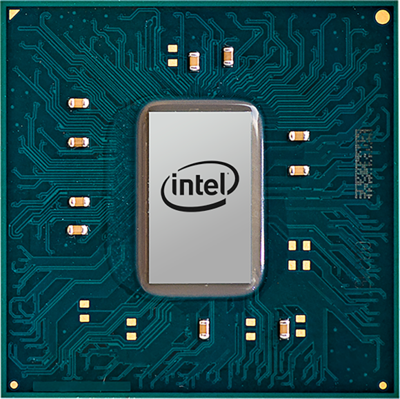
The Skylake CPU
The details about Skylake architecture has been very hard to find. Intel has been tight-lipped about the entire ordeal, forcing people to go through the block diagram and several other release materials and assume for the most part. Intel is said to reveal more details in their Development Forum later this month, but for now we will try to see what they have put inside this new architecture.
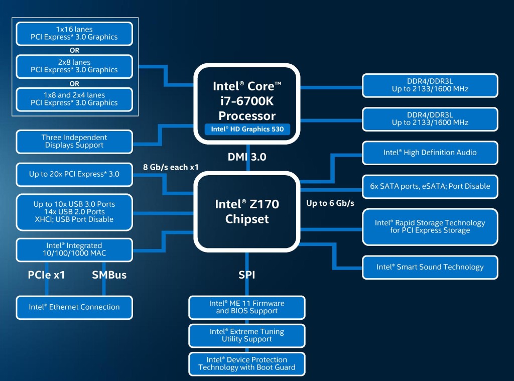
There are a couple of takeaways when you analyse this diagram. Firstly, the Skylake CPU features dual memory controllers for DDR4/DDR3L support. The available number of PCIe lanes from the CPu remains constant at sixteen, so that means devices can be used in PCIe 3.0×16, or x8/x8, or x8/x4/x4 if we are talking about feeding the PCIe slots from CPU only. With this configuration, we are looking at maximum of two-card SLI or three-card CrossFireX. But this problem is mitigated by the 20 PCIe lanes available from the Z170 PCH, so with the bandwidth sharing we can easily see Skylake enabling three+ card configurations.
We did talk about the upgraded DMI. Now in its third generation, the DMI 3.0 upgrades the speed of the CPU to chipset interconnect (a four-lane interface) from PCIe 2 to PCIe 3. That in theory is a speed bump of about 60%. The only caveat to DMI3.0 is that it requires the motherboard traces between the CPU and the chipset to be shorter by around 14% (7 inches compared to 8 inches in DMI2.0) to allow faster speeds. DMI3.0 brings with it the chipset connectivity, one of the biggest aces for the Z170 ecosystem.
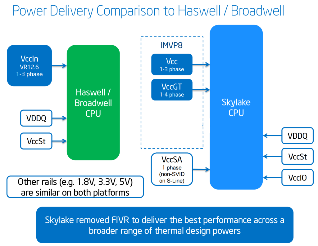
In our Haswell-E review, we talked about Intel’s move to create a fully integrated voltage regulator (FIVR) in the processor itself and how manufacturers used different means (OC Socket for example) to bypass those restrictions and add overclocking/stability features. The addition of FIVR meant cheaper motherboards since the manufacturers didn’t have to develop their own, but it also meant that there was an extra component inside the processor, and that contributed a great deal for the not-so-great thermal performance of both Haswell/Broadwell. With Skylake, the control is back on the motherboard again. This should reduce the temperature of the processor package a bit. The downside to this is slightly expensive motherboards and the possibility of seeing over-the-top solutions from manufacturers.
The Integrated graphics is now in its ninth generation, and again like the CPU architecture, details about it are as scarce as it can get. Intel calls the iGPU in Skylake GT530 (naming conventions are weird in Skylake; this can easily be mistaken as a NVidia DGPU) and it features a 24 EU design, running at 1150MHz. From multiple sources including AnandTech’s excellent review, the GPU design looks to be following Intel’s GT2 design and features three sub-slices of 8 EUs each. There are also some improvements under the hood here. The slices and the non-sliced areas feature individual power and clock domains, which allow an efficiency increase depending upon the workload.
Amongst other features we have support for memory colour stream compression which is again the reduction of transfer paths for small quantities of image and texture data. ‘Camera Pipe’ is introduced to make use of hardware acceleration to do standard adjustments to images. We will see more implementation of Camera Pipe in future, since it uses DX11 extensions and is teamed with SDKs for developers.
Z170 Chipset
By far the biggest feature for the Z170 chipset is its inclusion of a massive Flex-IO hub called HSIO. The numbers of Flex-IO ports that can flip between PCIe lanes/USB3.0 ports/SATA 6Gbps ports are bumped from 18 in Z97 to a whopping 26 in Z170.
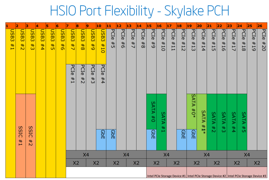
These 26 HSIO ports in Z170 are split according to their functionality – the first six are exclusive to USB 3.0, with two reserved for super-speed interconnects. The rest 20 are split into five groups supporting four PCIe 3.0 lanes each. The last three such sets are labelled as Intel PCIe Storage Device. We have already talked about the upgraded Intel RST now supporting up to three PCIe based storage devices and with this we will finally have RAID array between M.2 and SATA Express devices as long as they are connected and controlled via these HSIO ports/lanes.
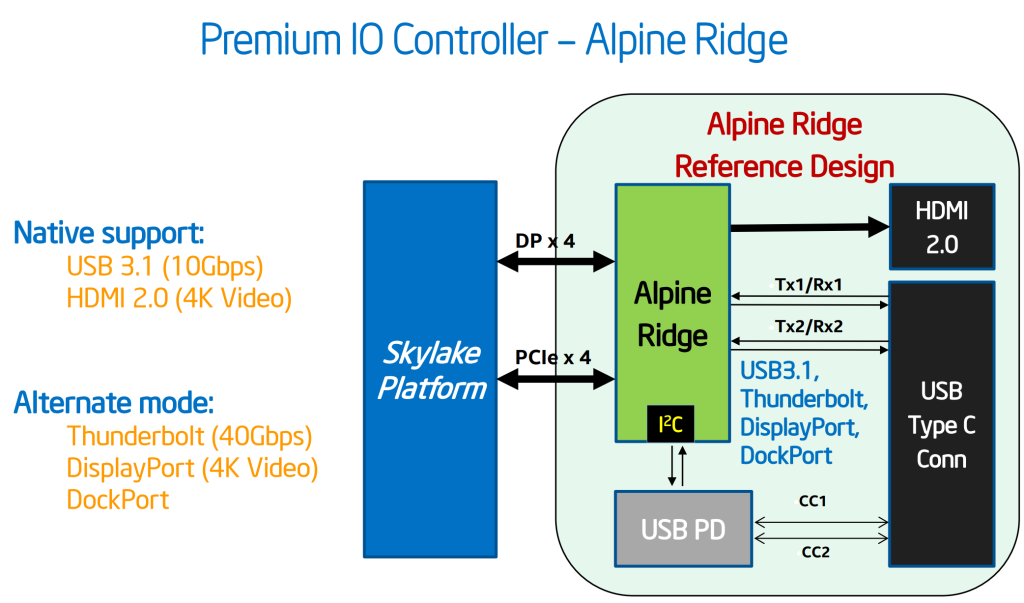
The Alpine Ridge Thunderbolt controller debuting with the Z170 chipset will use four PCIe lanes, and it supports USB3.1 Gen 2, Thunderbolt 3, DisplayPort and USB Type-C. It also has the ability to convert a DP signal to HDMI2.0.
The ASMedia ASM1142 controller on the other hand uses two PCIe lanes and should be the most common implementations on most motherboards to provide USB3.1 Gen 2 solutions since as of now the Alpine Ridge controller remains exclusive to some motherboard manufacturers.
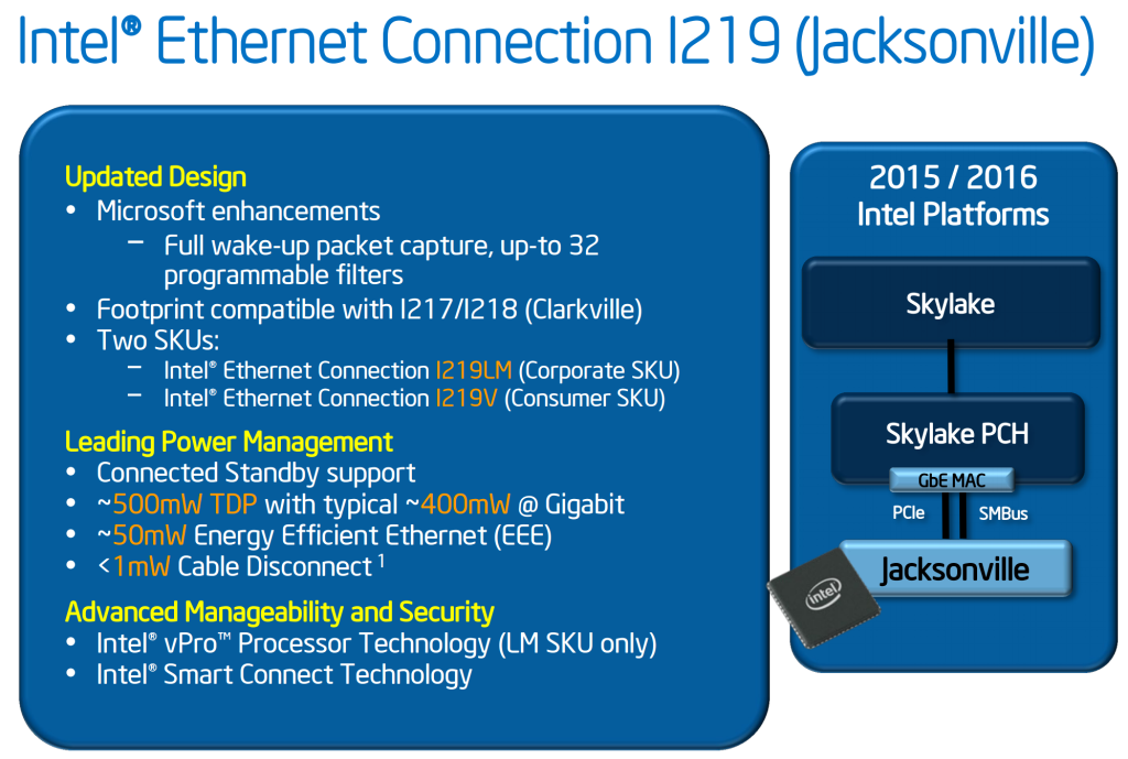 Also debuting is Intel’s new GbE controller, the I219. Dubbed Jacksonville, the I219 will be available in two flavours, I219-V for consumers and the more corporate grade I219-LM.
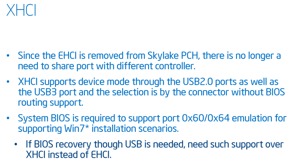
There are some improvements to power and PCIe signal routing under the hood, and the introduction of XHCI means that Z170 chipset and BIOS won’t support USB2.0 EHCI mode. The exclusion of EHCI mode can be frustrating for most users since it won’t allow Windows 7 installation via USB sticks. You will need to install the OS from optical media.
ASUS Z170-A Motherboard Visual analysis:
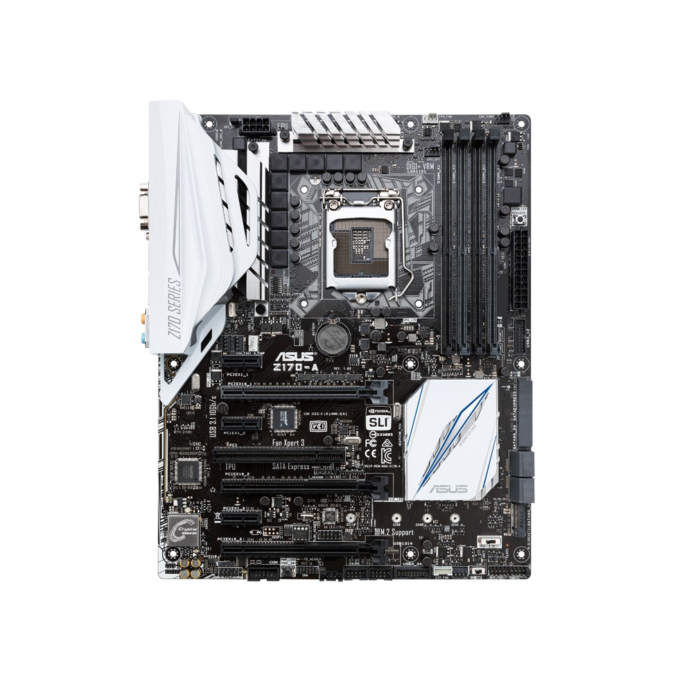
With the details about processor and chipset out of the way, let’s look at the launch board that ASUS has graciously provided us for testing. It’s dubbed Z170-A, and to those who are familiar with ASUS’ naming schemes would quickly understand that this represents ASUS’ mid-range consumer grade motherboard. That being said, on a pure visual basis the board looks anything but mid-range, with design cues taken directly from their X99 range. I had the chance to see the X99-A in person (Sumon reviewed it), and it doesn’t look as pleasant as the Z170-A. The closest that the Z170-A comes in terms of aesthetics is the X99-Deluxe, which features a similar white plastic cover over the silver bare I/O port tops. Unlike the X99-Deluxe the cover doesn’t extend to the audio section. Also worth noting that the VRM and PCH heatsinks are silver coloured.
 Starting from the left top corner, the 8pin CPU power connector sits between the top and the left VRM assemblies. Beside the power connector is a jumper called CPU_OV, which enables overvolting the CPU beyond the rated voltages that BIOS allows. The black chokes are visible in the power delivery section, and ten chokes, one for each phase translates into ten VRM phases. There are a total of seven four pin fan headers on the Z170-A, and three are in the top section of the motherboard. The CPU_FAN is white in colour, and near the right hand corner we have the CHA_FAN4 header. The CPU_OPT header is placed in the narrow space between the DIMM slot A1 and the top VRM assembly. The VRM is a ten-phase, all-digital affair featuring ASUS’ Digi+ VRM technology, which is in essence a combination of hardware and software to ensure proper voltage delivery on CPU, memory and PCH.
The CPU socket area is clean but ASUS continues to paint the PCB signal routes white around it, giving it a nice look. As stated before, the CPU cooler mounting holes remain the same 75mm apart in Z170 based motherboards as well, something that is good news for most people who don’t want to invest in a new cooler. Four DIMM slots are marked grey and black to indicate dual channel operation. The Z170-A supports up to 64GB of DDR4 memory with speeds of up to 3400MHz, though memories of that speed are crazily expensive and have no real benefit on every day performance. Intel’s new XMP profiles are also supported.
The top right hand side of the motherboard is mostly devoid of any ports or connectors. Continuing along the right hand edge, we have the memOK! Button, the 24pin power connector for the motherboard and an internal USB3.0 header.
The storage section of Z170-A has no surprises: six SATA 6Gbps ports, two occupied as part of a single SATA Express connector. All of them support RAID 0/1/5/10. Our test sample came with one of the SATA ports labelled OS Drive, implying that port to be used for the boot hard disc. There’s also an Ultra M.2 x4 connector on board right next to the SATA ports. It’s a Socket 3 connector and supports type 2242/2260/2280/22110 storage devices (both SATA & PCIE mode) and support PCIe RAID.
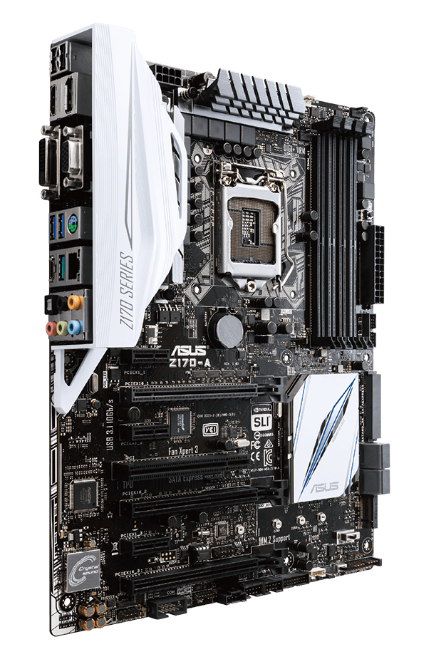 Next to the M.2 slot we have a TPU switch. The bottom section of the motherboard has the usual set of connectors and some new additions. From right to left, there are front panel connectors, the clear CMOS jumper, the EZ XMP switch to flick XMP on/off, a four pin fan header (CHA_FAN3), the EXT_FAN connector for the external fan hub card (that debuted with the X99-Deluxe), another internal USB3.0 header, two USB2.0 headers, the Thunderbolt and COM headers, a Power Switch (thankfully!) and the front panel audio header. Between the last PCIe slots there is the BIOS Flashback header, and a lone VBOOT_TEST header is between the PCI slot and the second PCIe x16 slot.
For PCIe expansion, the Z170-A comes equipped with three full-length PCIe 3.0 x16 slots. Only the top two are electrically wired as x16 though, and the last PCIe x16 slot supports a max of x4 mode and shares bandwidth with the SATA ports 5 & 6. The board also has three PCIe 3.0 x1 slots and a PCI slot for legacy products (Audio cards/RAID cards).
Like ASUS’ most recent boards, the audio section has a separate PCB and full EMI shielding, and the path of separation is lit by a white (yellowish) LED. The Crystal Sound 3 is built upon an upgraded Realtek ALC892 codec. The gold Nichicon audio capacitors are visible near the Crystal Sound 3 chip. The audio features include Absolute Pitch 192kHz/24-bit True BD Lossless Sound, DTS Connect/DTS Studio Sound and audio amplification for headphones and speakers.
Above the first PCIe x1 slot we have three more fan headers, two of them black and one of them white. The white one is interesting since it is labelled W_PUMP, indicating that this is capable of running and controlling pumps for AIO liquid coolers or custom liquid cooling.
Coming to the I/O, ASUS has moved the PS/2 connector to the middle of the array. From left to right we have two USB2.0 ports, video output connectors including a DisplayPort, a HDMI, a VGA and a DVI-D connector, the PS/2 keyboard mouse combo port, two USB3.0 ports, the Intel GbE connector (courtesy the I219-V network controller dubbed Jacksonville), two USB3.1 Gen 2 ports (one Type-A and the other Type-C) and the usual assortment of audio connectors.
Accessories/in the box:
The following accessories are included with the Z170-A:
With the launch of Z170, we see the BIOS/UEFI evolve too to take advantage of the added features. ASUS for their Z170 boards have given the BIOS a new paintjob. The Z170 UEFI now has a black and cyan livery with the top right hand and bottom left hand corners sporting designs akin to the motherboard signal routes. That overall presents a very slick aesthetic, but it’s not all about the looks; once we delve deep in the UEFI we see the improvements that Z170 has brought about.
The first screen in UEFI is always the ‘easy mode’. For ASUS, that means an entire screen filled with information as small as system time and date to important ones such as CPU Temperature, Core Voltage and Boot Sequence. From Z97 we are also getting XMP profile switching options, Intel RST options and a more updated fan profile setting. From there, one can choose EZ System Tuning which automatically selects the best settings for the current system, ranging from CPU clock speeds/DRAM frequency to the system fan profiles. The QFan Control is there to select custom fan speed/temperature curves.
Pressing F7 opens the traditional UEFI or advanced options. The main tabs have remained the same. Let’s look at them one by one.
My Favorites : This is for quick access of the most used settings without searching for them in the heaps of things available.
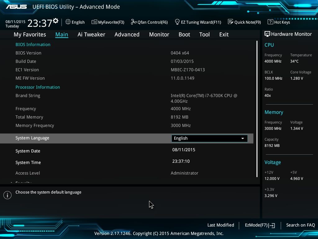
Main : Presents essential information about the BIOS, Processor, Memory, System Time/Date/Language. Also has the option to set administrator passwords for the UEFI.
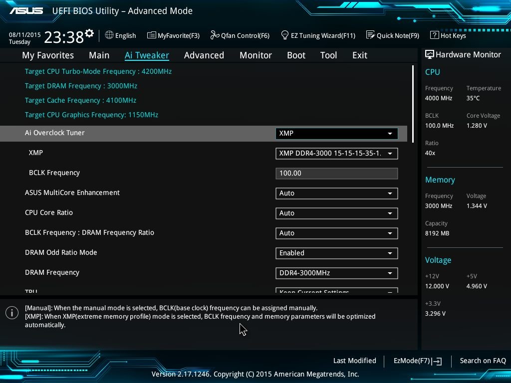
Ai Tweaker: This is the main page for tweaking and overclocking the processor and memory. With Skylake, we see the advent of newer options like BCLK-DRAM frequency ratio. This being a mainstream board (read non-ROG) the options available are still not borderline crazy, but there are enough things for a seasoned overclocker to play with.
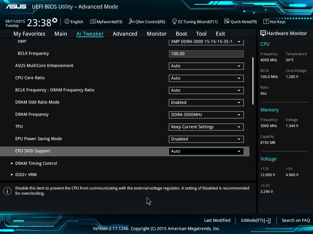
An interesting option here is the option to select CPU SVID support, which when enabled opens the route for the CPU to communicate with the external voltage regulator.
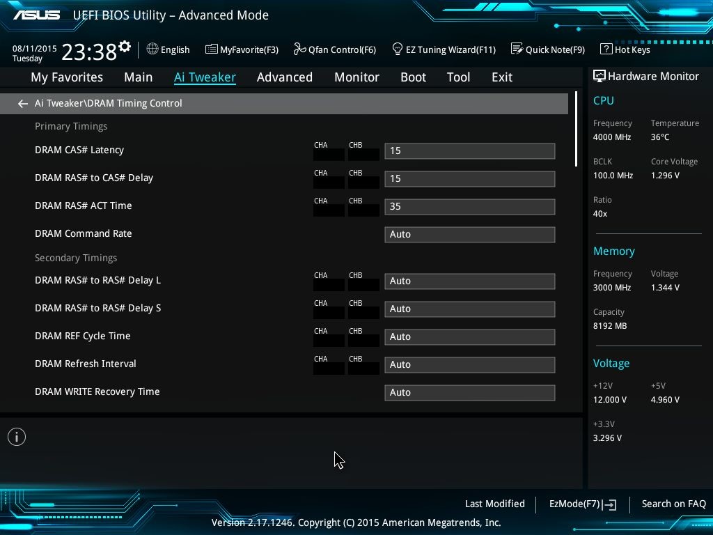
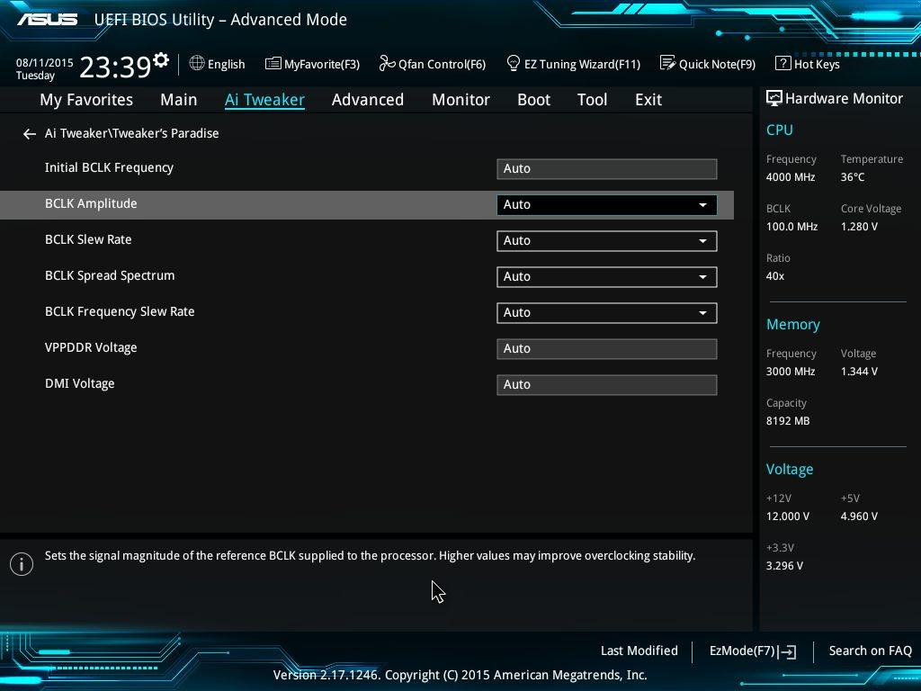
Delving deeper into Ai Tweaker we see options to set individual timings for memory. The CPU sections are extensive too and now contain a slew of options dedicated to BCLK.
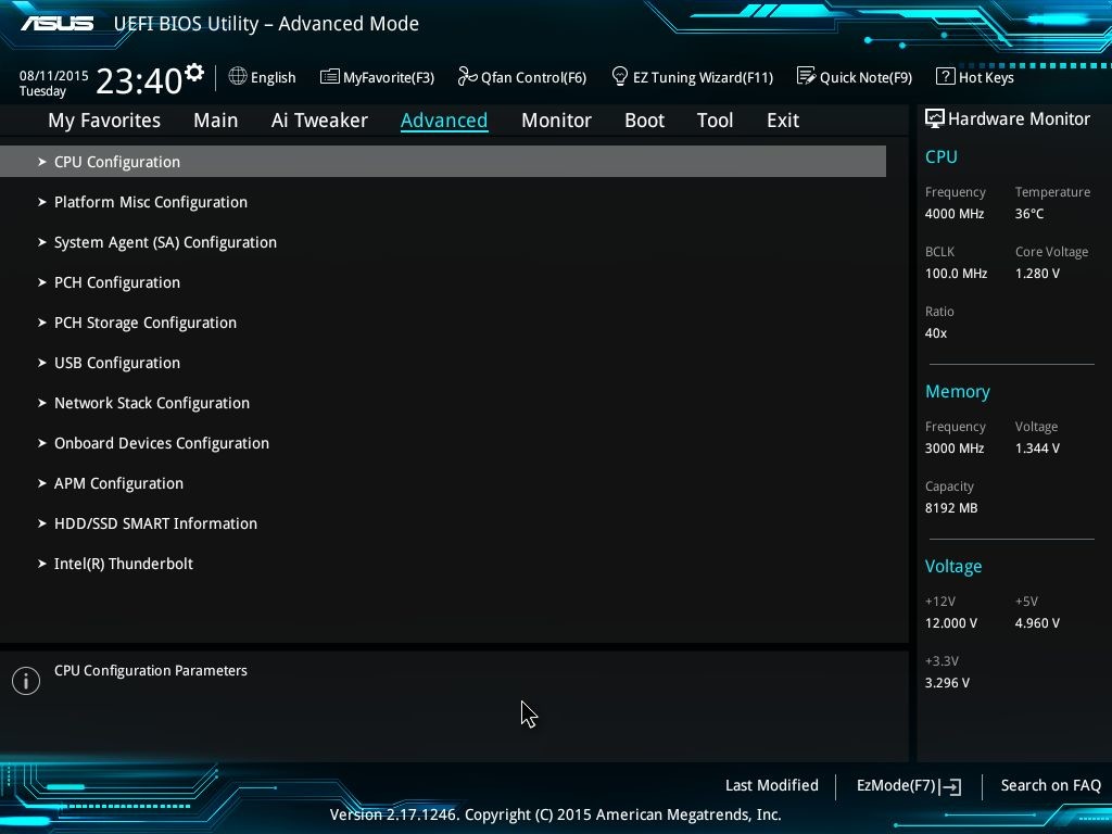
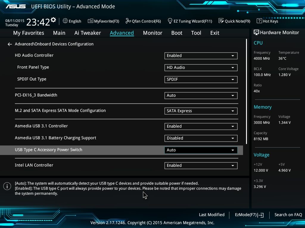
Advanced: Contains settings related to CPU (Power), System Agent, Network Stack, USB, PCH, Onboard Devices etc.
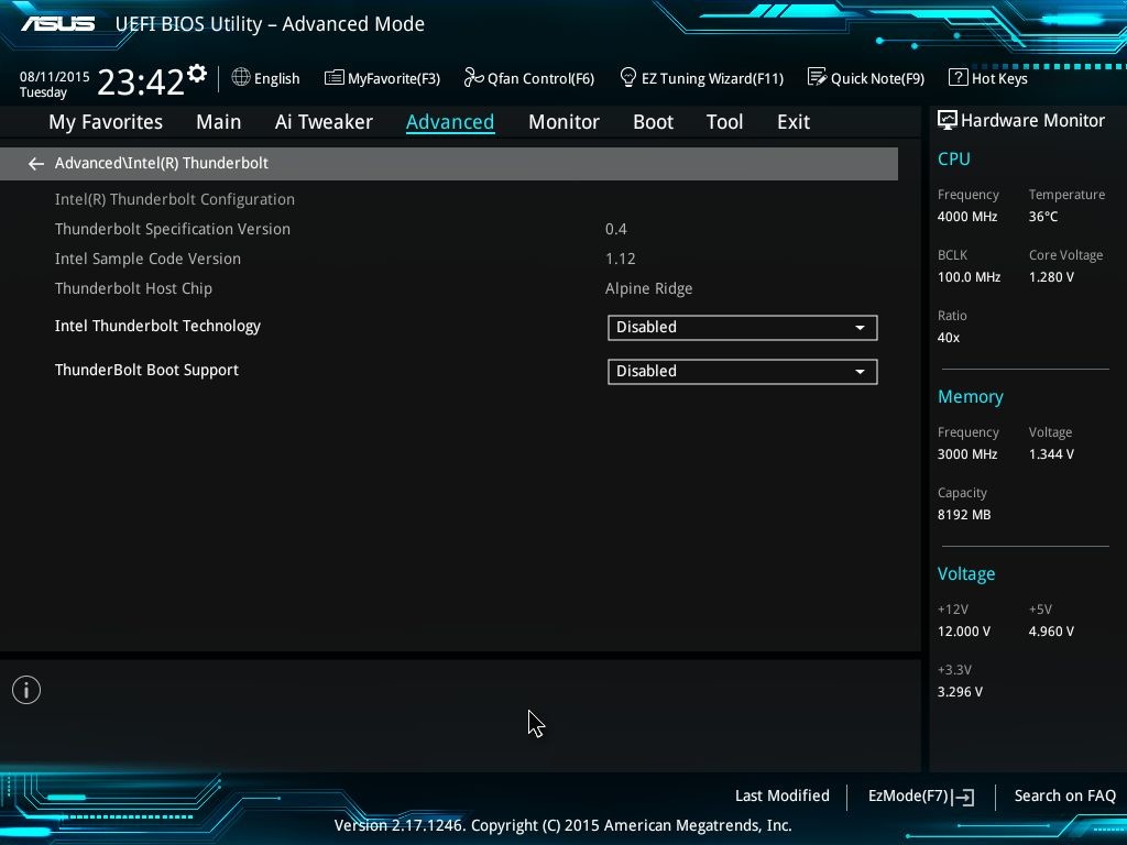
A new addition here is Intel Thunderbolt related options. Thunderbolt is enabled by the Alpine Ridge controller from Intel, and here we can see the specification versions as well as options to boot from a Thunderbolt device.
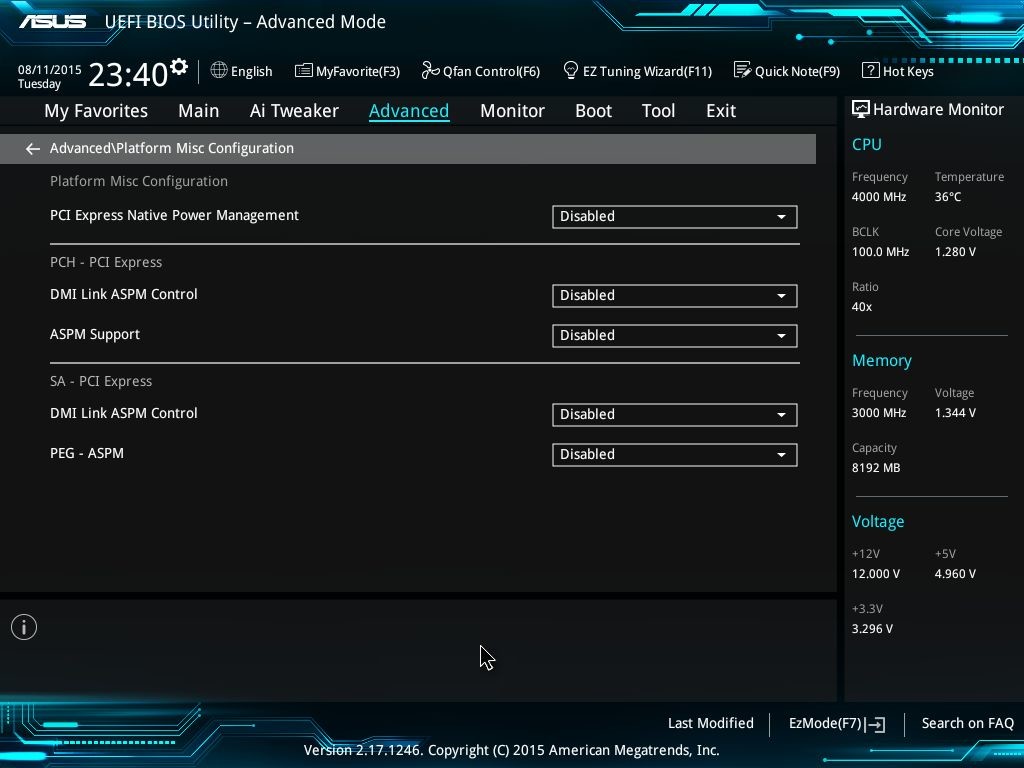
In Platform configuration there are options to select DMI Link settings. The maximum link speed can also be selected from here.
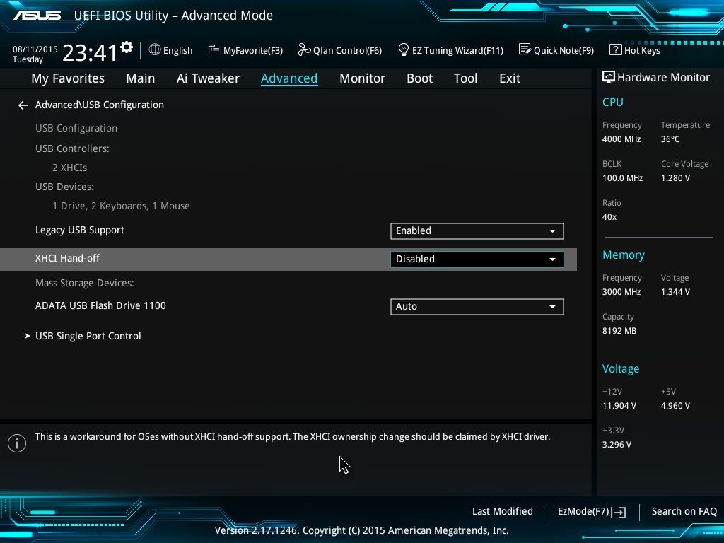
USB configuration contains settings for newer supported technologies such as XHCI. Settings for USB Type C can also be found in the Advanced section.
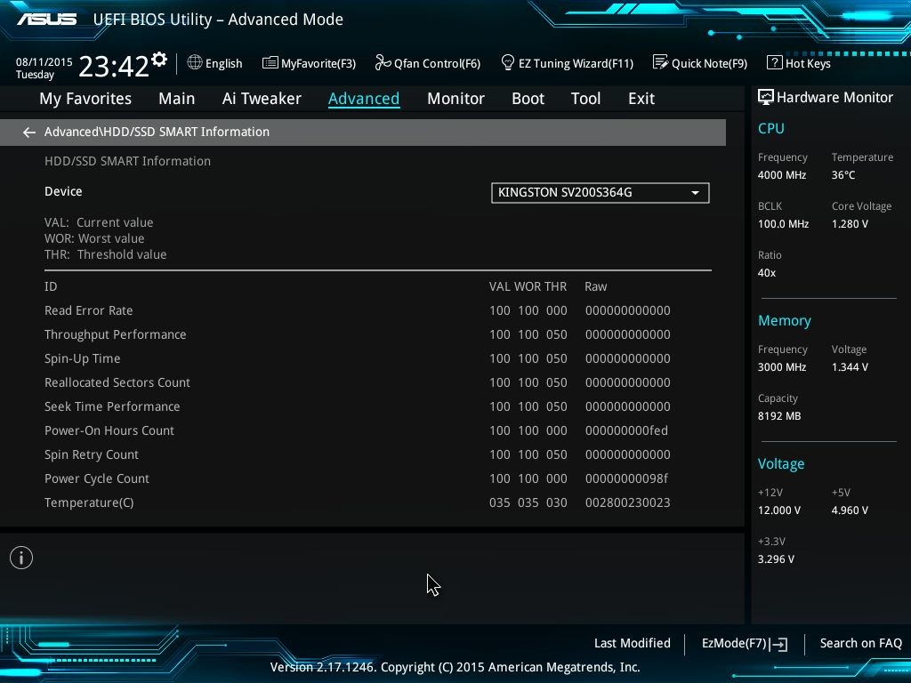
You also get information about SMART supported hard disc drives.
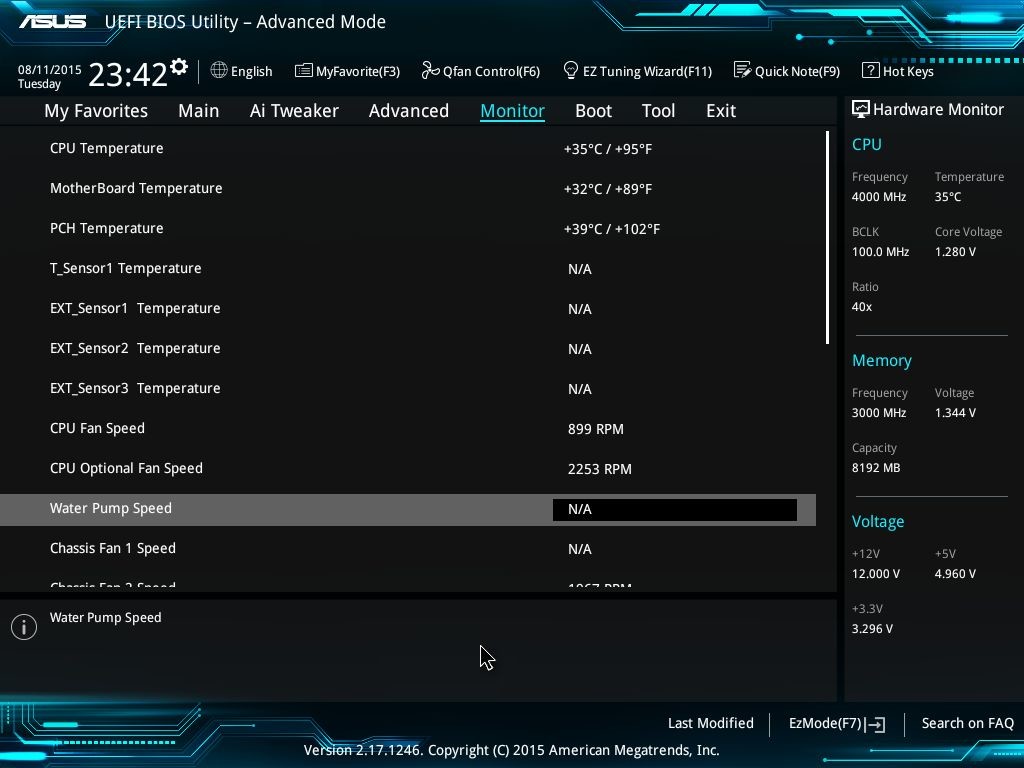
Monitor: Temperature/Voltage/Fan speeds can be monitored from here. ASUS has added Water Pump Speed/Control in this menu.
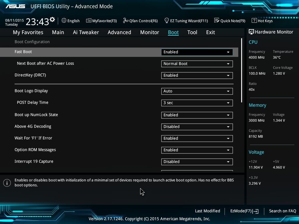
Boot: Regular boot sequence/override options.
Tools: There are a couple of UEFI tools that ASUS provide with the Z170-A.
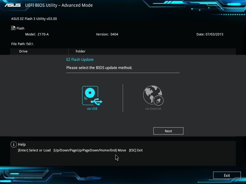
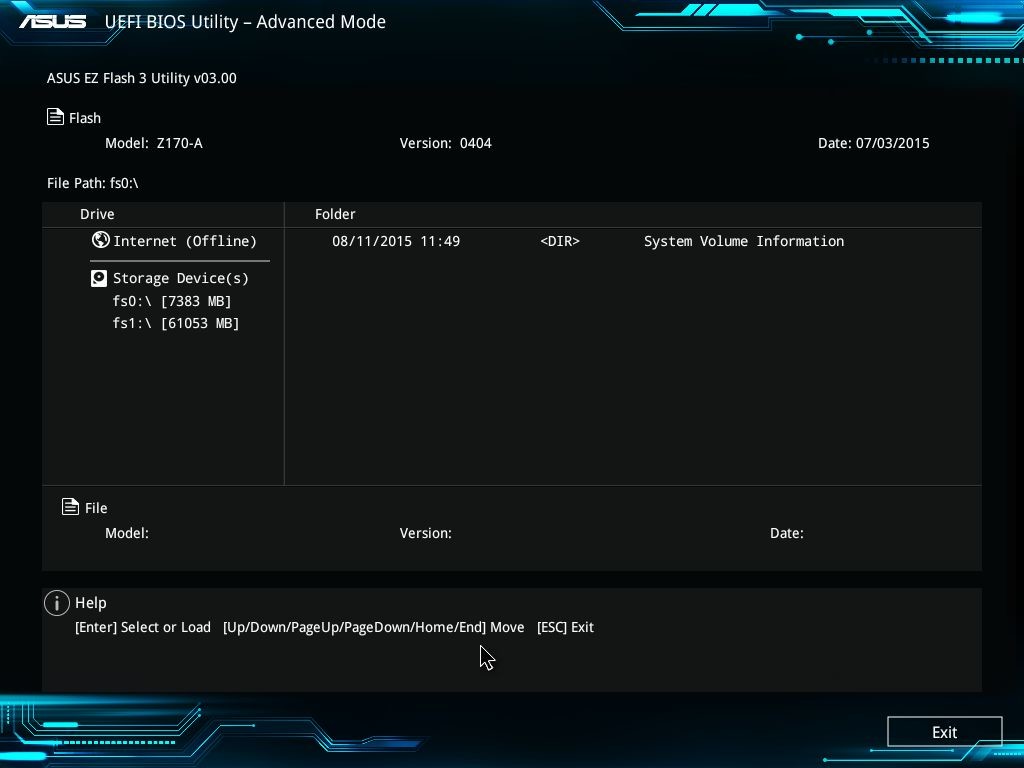
EZ Flash 3 is their BIOS update tool which can now update directly from the internet or via a properly formatted USB stick containing the .CAP file.
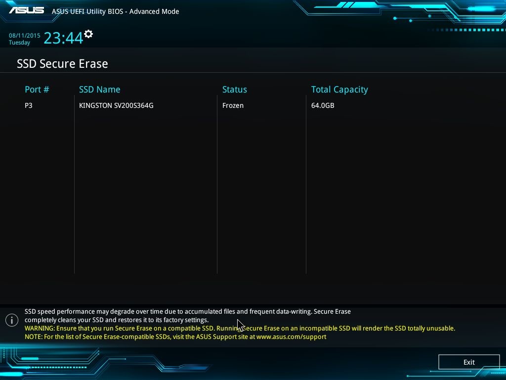
SSD Secure Erase can format a SSD from the BIOS. This is especially helpful for new/malfunctioning SSDs that cannot boot into an OS, though ASUS says that only compatible SSDs should be used for this feature.
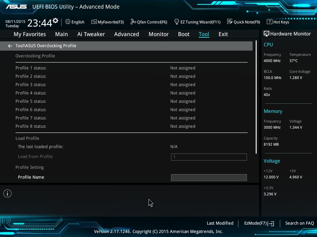
ASUS Overclocking Profile lets users save a custom profile which can then be accessed later to load the values.
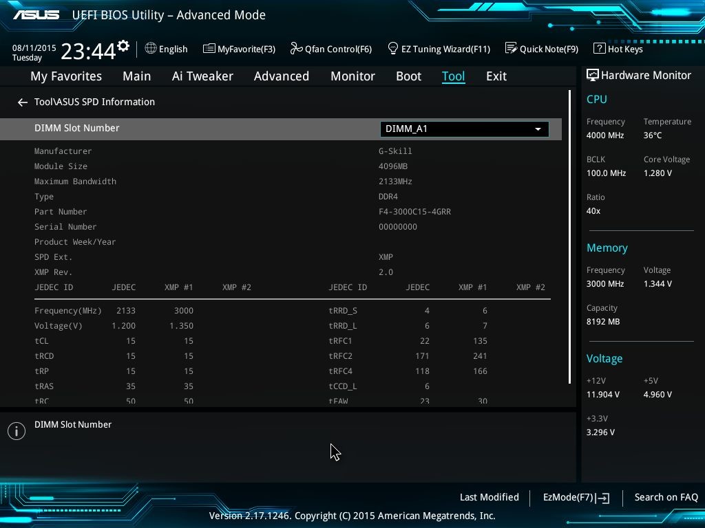
ASUS SPD information provides details about installed DRAM kits, including JDEC supported timings and XMP values.
Software walkthrough:
ASUS’ software implementation has always been centred on their AI Suite utility, a central hub for their other programs/software to function. I ran into some issues with the Z170-A where I couldn’t install AI Suite 3, so I thought to cover other software that came aboard. I will be covering AI Suite for Skylake in a future review.
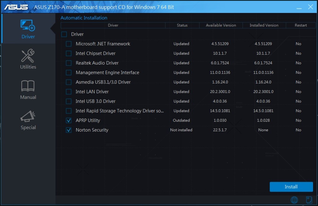
The installer has received the same paintjob as that of the UEFI. ASUS splits the bundle into drivers, utilities and then added software bonuses. Added third-party software include Daemon Tools Pro, an imaging software, WinZip, Chrome Browser and Norton Security.
Turbo LAN is ASUS’ custom network prioritizing and monitoring software built on top of cFOS LAN.
ASUS Boot Setting provides an option to directly boot into BIOS without pressing a button. There are also options for fast boot and wake after sudden power loss.
Test Setup:
The following test system was used for this review:
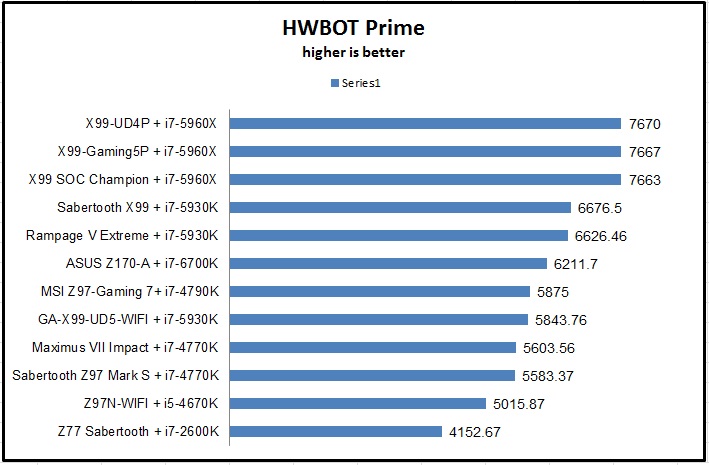
Benchmarks:
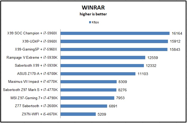
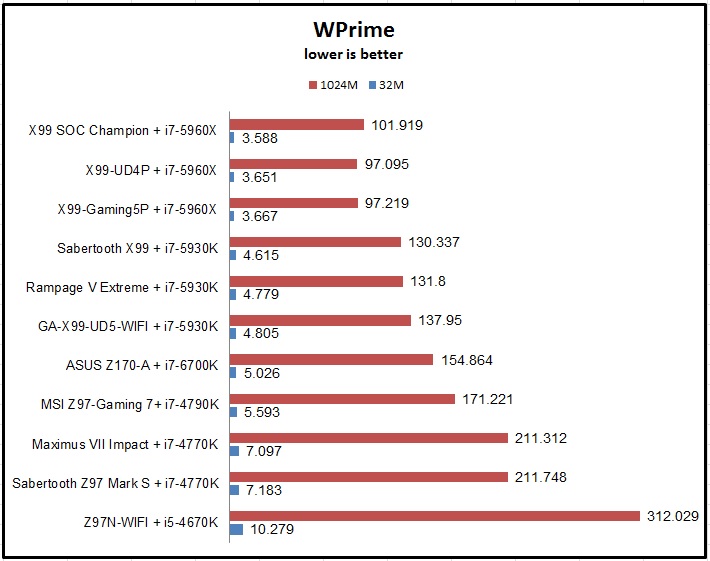
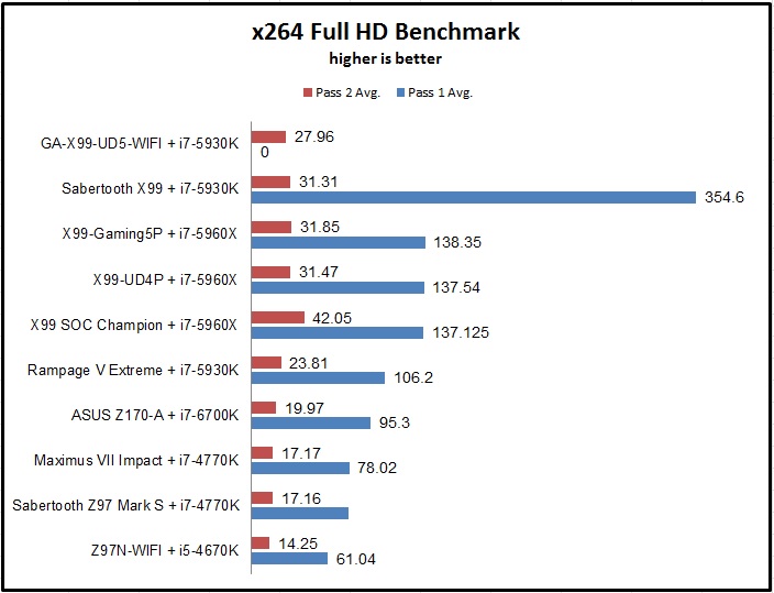
I compared the i7-6700K with the earlier motherboards I had reviewed. I also took two of my friends’ help to get some data about the i7-2600K and i7-4790K. A keen eye can easily observe that not all benchmark numbers were collected for these two processors, but in most of the benchmarks I have tried to include them to see the performance difference between two generations.
Let’s fire up our usual suite of benchmarks first.
3D Particle Movement is a benchmark penned by Dr.Ian Cutress (Lead Reviewer, AnandTech) and it works by taking basic 3D movement algorithms used in Brownian Motion simulations and testing them for speed. High floating point performance, MHz and IPC wins in the single thread version, whereas the multithread version has to handle the threads and loves more cores.
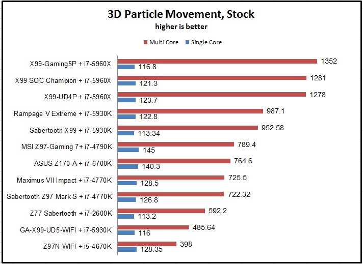 Here we see an interesting start for the 6700K. While it trumps the 4770K by 5%, it trails the newer 4790K by 3%.
Next up is Cinebench in its three most popular variants. Cinebench is a popular rendering program.
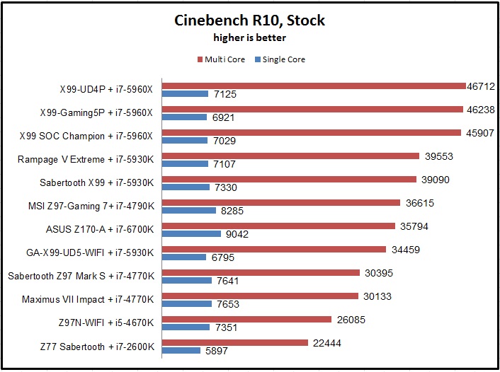
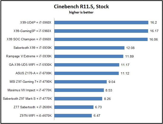
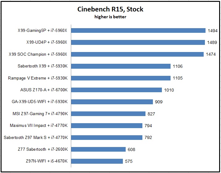 In R10, the 6700K trails the 4790K by 2%, but in R11.5 and R15 comes back with a strong showing. In Cinebench R15, Skylake’s lead is an astonishing 22%.
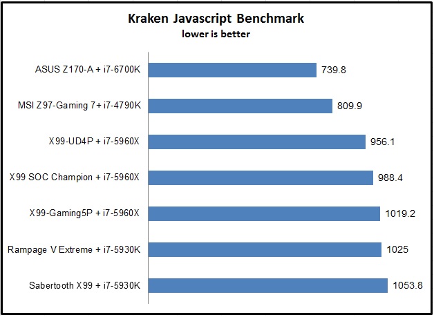
I started to include Web based benchmarks quite some time back in my review. While most of them utilize JavaScript, they run a variety of tests which can stress your system quite hard.
Kraken is Mozilla’s well-known benchmark that measures the speed of several different test cases extracted from real-world applications and libraries. The overall layout is built on SunSpider, another popular JavaScript based benchmark.
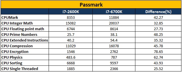
 Lastly, I fired up Passmark to compare between the i7-6700K and the i7-2600K. The difference in performance is noted down with each benchmark. The newer processor humbles the older one, and in some cases the difference is shocking. In CPU Encryption, the 6700K is almost 80% faster than the Sandy Bridge part 2600K.
Overclocking:
As for the overclocking, I took two routes to see how the chip and the board fared. The first amongst them was simple multiplier based overclocking where I didn’t touch BCLK settings and played with VCore and multipliers. The second was purely on BCLK based settings.
For the i7-6700K, the maximum overclock achieved through multipliers was 4.8GHz at 1.35v VCore with 100MHz BCLK and 48x multiplier.
For the i7-6700K, the maximum overclock achieved through multipliers was 4.6GHz at 1.35v VCore with 200MHz BCLK and 23x multiplier.
Conclusion:
I think Skylake demands a conclusion of its own. In this review, we have covered its flagship desktop part, the Core i7-6700K. With desktop Broadwell as elusive as the Bigfoot, our best chance to analyse performance of Intel’s 14nm parts. Intel had a couple of things to consider when it moved to its next generation of processors. Firstly, per-generation performance yield was in single digit percentages. Secondly, with each new generation the general overclocking potential for a consumer-grade chip went down by a notch. Lastly, since Ivy Bridge, Intel processors have been plagued with thermal issues, and a majority of it hovered around Intel’s choice of TIM. While I cannot conclude about Skylake’s other representatives, the Core i7-6700K, performance wise, is a mixed bag. In some tests it bests Intel’s 4790K by quite some margin, and in some it loses to it. It wins more than it loses, however. When compared to even older i7-2600K, the performance gap is larger across the board. In some tests the performance increase is 50%. People with Sandy Bridge systems will definitely see a nice boost in overall performance. For Haswell and above, the upgrade may not be worth it if you are only considering raw CPU performance.
But the real gem is the Z170 chipset itself. Intel has introduced a lot of new features with its Alpine Ridge controller, providing 26 PCIe lanes via its HSIO plus USB3.1 Gen2, Thunderbolt and DisplayPort to name a few. That means no PCIe bandwidth issues – M.2 and SATA Express can be used at once. Updated DMI means faster interconnect between CPU and PCH, and Intel’s RST upgrades mean three plus PCIe storage devices can be used in RAID. Intel’s Jacksonville network controller debuts with Z170 as well; in essence significantly upping the ante for Skylake based systems.
Let’s look at the motherboard then. ASUS’ Z170-A represents their (arguably) lowest end of the mainstream range, but the feature sets provided with this board left me baffled about its pricing. The Z170-A will be retailing for Rs.14775 (Plus taxes). While this is lower than what I expected, the entire sub-20K INR range is a segment fiercely contested by other brands. It may also come into direct competition with its ROG brethren. Aesthetic wise, this is a clear departure from ASUS’ Z97 boards and more in line with their X99 setup. Feature wise, you get a ten phase fully digital VRM, onboard Power and XMP switches, six SATA 6Gbps ports, a full x4 M.2 slot, three PCIe x16 slots (though the last one is wired x4), bunch of USB3.0 internal headers and external ports, two USB3.1 Gen2 ports in both flavours (Type-A and Type-C) via the AsMedia controller and EMI shielded audio courtesy of Crystal Sound 3. Adding to the mix ASUS’ upgraded UEFI that offers more features in a mainstream board like the Z170-A and their fully decked out software bundle, the entire package is very lucrative. The overclocking performance was pleasantly surprising as well, with my i7 sample reaching 4.8GHz with an AIO liquid cooler. My only gripes are the lack of an on-board LED debug display and any wireless connectivity. But then I may be asking for too much. With good looks and performance to match, ASUS’ Z170-A might be the first strike that the company needs. Whether it can reign supreme will be seen shortly.
The Z170-A deserves a gold award for its performance, aesthetics and the complete bundle it provides. With the new chipset, ASUS has stuck with what worked best for them and then matured the ecosystem of UEFI and software. The upgraded hardware has made its way into the first member of the mainstream league, bringing along good performance across the board. When you consider the price, it looks even more value for money. For Skylake, my complete conclusion will be out once I test the Core-i5 variant as well, but for now, if you are using Haswell/Devil’s Canyon, the only reason you should choose Intel’s 14nm processor is for the chipset itself. And oh, if you love BCLK based overclocking, that is.
What’s new with Skylake?
Before we delve into the technical details, let’s first look at the most immediate change: retail packaging. The desktop Skylake chips will be using a colourful box, a stark departure from the monotonous blue/black boxes that Intel has been offering. As of now we get to see two box-shots, though it is safe to assume that with the release of more processors, we will see a variety of packaging for Skylake.
The Skylake CPU
The details about Skylake architecture has been very hard to find. Intel has been tight-lipped about the entire ordeal, forcing people to go through the block diagram and several other release materials and assume for the most part. Intel is said to reveal more details in their Development Forum later this month, but for now we will try to see what they have put inside this new architecture.
There are a couple of takeaways when you analyse this diagram. Firstly, the Skylake CPU features dual memory controllers for DDR4/DDR3L support. The available number of PCIe lanes from the CPu remains constant at sixteen, so that means devices can be used in PCIe 3.0×16, or x8/x8, or x8/x4/x4 if we are talking about feeding the PCIe slots from CPU only. With this configuration, we are looking at maximum of two-card SLI or three-card CrossFireX. But this problem is mitigated by the 20 PCIe lanes available from the Z170 PCH, so with the bandwidth sharing we can easily see Skylake enabling three+ card configurations.
We did talk about the upgraded DMI. Now in its third generation, the DMI 3.0 upgrades the speed of the CPU to chipset interconnect (a four-lane interface) from PCIe 2 to PCIe 3. That in theory is a speed bump of about 60%. The only caveat to DMI3.0 is that it requires the motherboard traces between the CPU and the chipset to be shorter by around 14% (7 inches compared to 8 inches in DMI2.0) to allow faster speeds. DMI3.0 brings with it the chipset connectivity, one of the biggest aces for the Z170 ecosystem.
In our Haswell-E review, we talked about Intel’s move to create a fully integrated voltage regulator (FIVR) in the processor itself and how manufacturers used different means (OC Socket for example) to bypass those restrictions and add overclocking/stability features. The addition of FIVR meant cheaper motherboards since the manufacturers didn’t have to develop their own, but it also meant that there was an extra component inside the processor, and that contributed a great deal for the not-so-great thermal performance of both Haswell/Broadwell. With Skylake, the control is back on the motherboard again. This should reduce the temperature of the processor package a bit. The downside to this is slightly expensive motherboards and the possibility of seeing over-the-top solutions from manufacturers.
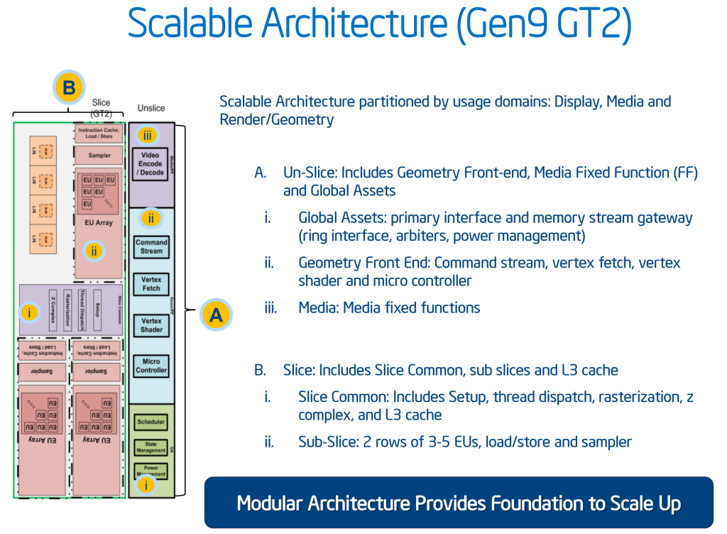
The Integrated graphics is now in its ninth generation, and again like the CPU architecture, details about it are as scarce as it can get. Intel calls the iGPU in Skylake GT530 (naming conventions are weird in Skylake; this can easily be mistaken as a NVidia DGPU) and it features a 24 EU design, running at 1150MHz. From multiple sources including AnandTech’s excellent review, the GPU design looks to be following Intel’s GT2 design and features three sub-slices of 8 EUs each. There are also some improvements under the hood here. The slices and the non-sliced areas feature individual power and clock domains, which allow an efficiency increase depending upon the workload.
There is also a feature called Multi Plane Overlay which adds fixed function hardware to the display controller to bypass the redundant redirection of data while the 3D engine operates on an image. This in turn means that the default CPU->DRAM->GPU->DRAM->Display Controller path for the data is reduced for faster and more efficient operation. This feature will be supported on Win 8.1 and above with Skylake’s iGPU.Amongst other features we have support for memory colour stream compression which is again the reduction of transfer paths for small quantities of image and texture data. ‘Camera Pipe’ is introduced to make use of hardware acceleration to do standard adjustments to images. We will see more implementation of Camera Pipe in future, since it uses DX11 extensions and is teamed with SDKs for developers.
The Skylake iGPU also gets a bunch of media encoding/decoding features, and HEVC support comes in the form of a full, low power fixed function HEVC decoder. JPEG encoding upto 16K*16K is supported. In terms of outputs, the iGPU gets rid of the VGA video connector, so any analog (VGA) display output you see in a Skylake motherboard isn’t fed from the iGPU, but from an active DAC chip on board.Z170 Chipset
By far the biggest feature for the Z170 chipset is its inclusion of a massive Flex-IO hub called HSIO. The numbers of Flex-IO ports that can flip between PCIe lanes/USB3.0 ports/SATA 6Gbps ports are bumped from 18 in Z97 to a whopping 26 in Z170.
These 26 HSIO ports in Z170 are split according to their functionality – the first six are exclusive to USB 3.0, with two reserved for super-speed interconnects. The rest 20 are split into five groups supporting four PCIe 3.0 lanes each. The last three such sets are labelled as Intel PCIe Storage Device. We have already talked about the upgraded Intel RST now supporting up to three PCIe based storage devices and with this we will finally have RAID array between M.2 and SATA Express devices as long as they are connected and controlled via these HSIO ports/lanes.
The Alpine Ridge Thunderbolt controller debuting with the Z170 chipset will use four PCIe lanes, and it supports USB3.1 Gen 2, Thunderbolt 3, DisplayPort and USB Type-C. It also has the ability to convert a DP signal to HDMI2.0.
The ASMedia ASM1142 controller on the other hand uses two PCIe lanes and should be the most common implementations on most motherboards to provide USB3.1 Gen 2 solutions since as of now the Alpine Ridge controller remains exclusive to some motherboard manufacturers.
There are some improvements to power and PCIe signal routing under the hood, and the introduction of XHCI means that Z170 chipset and BIOS won’t support USB2.0 EHCI mode. The exclusion of EHCI mode can be frustrating for most users since it won’t allow Windows 7 installation via USB sticks. You will need to install the OS from optical media.
ASUS Z170-A Motherboard Visual analysis:
With the details about processor and chipset out of the way, let’s look at the launch board that ASUS has graciously provided us for testing. It’s dubbed Z170-A, and to those who are familiar with ASUS’ naming schemes would quickly understand that this represents ASUS’ mid-range consumer grade motherboard. That being said, on a pure visual basis the board looks anything but mid-range, with design cues taken directly from their X99 range. I had the chance to see the X99-A in person (Sumon reviewed it), and it doesn’t look as pleasant as the Z170-A. The closest that the Z170-A comes in terms of aesthetics is the X99-Deluxe, which features a similar white plastic cover over the silver bare I/O port tops. Unlike the X99-Deluxe the cover doesn’t extend to the audio section. Also worth noting that the VRM and PCH heatsinks are silver coloured.
The CPU socket area is clean but ASUS continues to paint the PCB signal routes white around it, giving it a nice look. As stated before, the CPU cooler mounting holes remain the same 75mm apart in Z170 based motherboards as well, something that is good news for most people who don’t want to invest in a new cooler. Four DIMM slots are marked grey and black to indicate dual channel operation. The Z170-A supports up to 64GB of DDR4 memory with speeds of up to 3400MHz, though memories of that speed are crazily expensive and have no real benefit on every day performance. Intel’s new XMP profiles are also supported.
The top right hand side of the motherboard is mostly devoid of any ports or connectors. Continuing along the right hand edge, we have the memOK! Button, the 24pin power connector for the motherboard and an internal USB3.0 header.
The storage section of Z170-A has no surprises: six SATA 6Gbps ports, two occupied as part of a single SATA Express connector. All of them support RAID 0/1/5/10. Our test sample came with one of the SATA ports labelled OS Drive, implying that port to be used for the boot hard disc. There’s also an Ultra M.2 x4 connector on board right next to the SATA ports. It’s a Socket 3 connector and supports type 2242/2260/2280/22110 storage devices (both SATA & PCIE mode) and support PCIe RAID.
For PCIe expansion, the Z170-A comes equipped with three full-length PCIe 3.0 x16 slots. Only the top two are electrically wired as x16 though, and the last PCIe x16 slot supports a max of x4 mode and shares bandwidth with the SATA ports 5 & 6. The board also has three PCIe 3.0 x1 slots and a PCI slot for legacy products (Audio cards/RAID cards).
Like ASUS’ most recent boards, the audio section has a separate PCB and full EMI shielding, and the path of separation is lit by a white (yellowish) LED. The Crystal Sound 3 is built upon an upgraded Realtek ALC892 codec. The gold Nichicon audio capacitors are visible near the Crystal Sound 3 chip. The audio features include Absolute Pitch 192kHz/24-bit True BD Lossless Sound, DTS Connect/DTS Studio Sound and audio amplification for headphones and speakers.
Above the first PCIe x1 slot we have three more fan headers, two of them black and one of them white. The white one is interesting since it is labelled W_PUMP, indicating that this is capable of running and controlling pumps for AIO liquid coolers or custom liquid cooling.
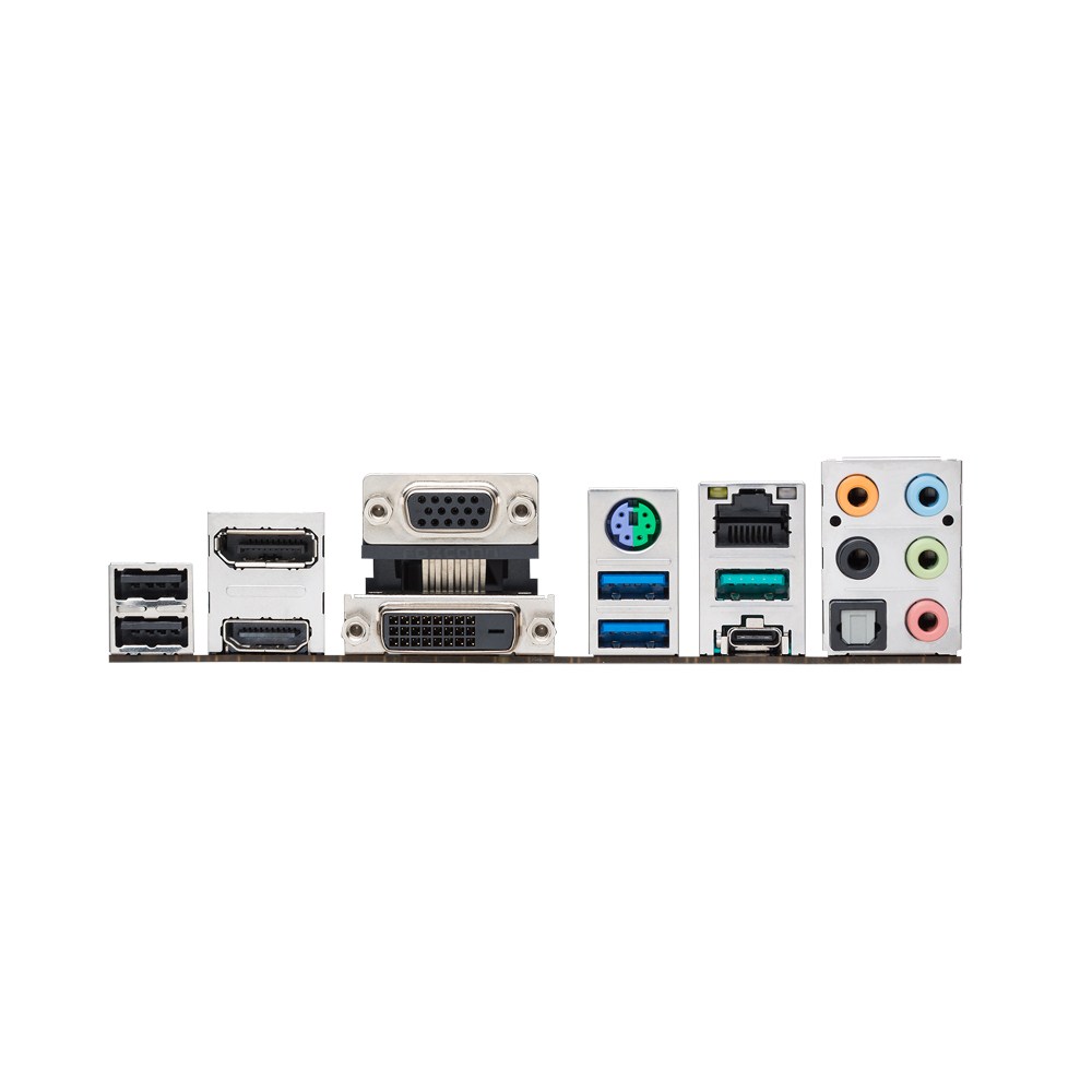
Coming to the I/O, ASUS has moved the PS/2 connector to the middle of the array. From left to right we have two USB2.0 ports, video output connectors including a DisplayPort, a HDMI, a VGA and a DVI-D connector, the PS/2 keyboard mouse combo port, two USB3.0 ports, the Intel GbE connector (courtesy the I219-V network controller dubbed Jacksonville), two USB3.1 Gen 2 ports (one Type-A and the other Type-C) and the usual assortment of audio connectors.
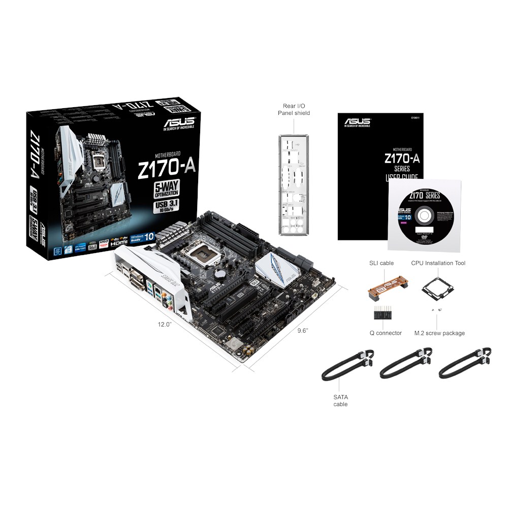
Accessories/in the box:
The following accessories are included with the Z170-A:
- User’s manual
- I/O Shield
- 3 x SATA 6Gb/s cable(s)
- 1 x M.2 Screw Package
- 1 x CPU installation tool
- 1 x SLI bridge(s)
- 1 x Q-connector(s) (1 in 1)
With the launch of Z170, we see the BIOS/UEFI evolve too to take advantage of the added features. ASUS for their Z170 boards have given the BIOS a new paintjob. The Z170 UEFI now has a black and cyan livery with the top right hand and bottom left hand corners sporting designs akin to the motherboard signal routes. That overall presents a very slick aesthetic, but it’s not all about the looks; once we delve deep in the UEFI we see the improvements that Z170 has brought about.
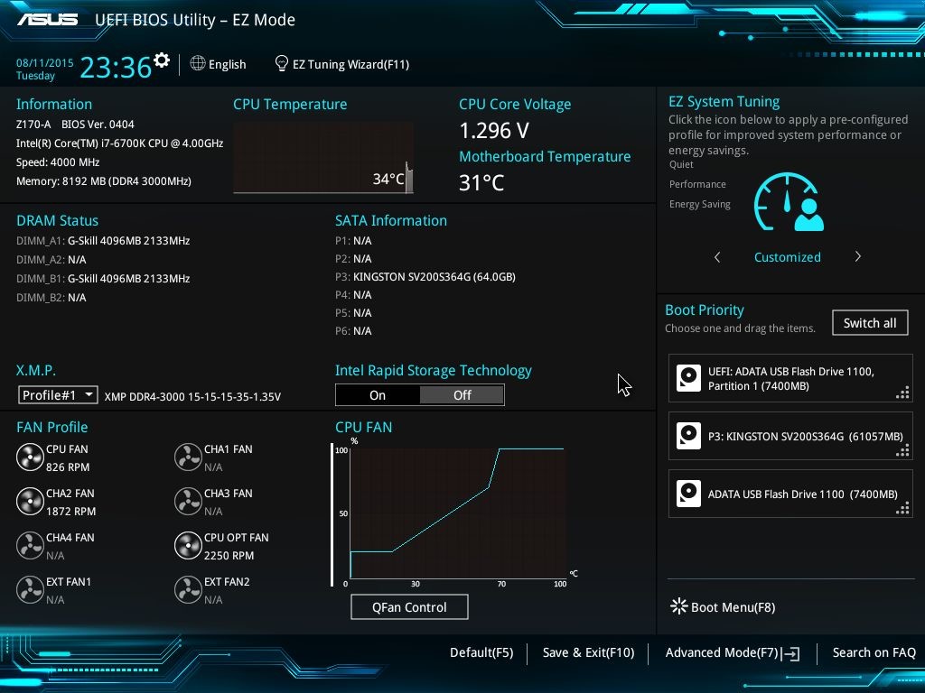
The first screen in UEFI is always the ‘easy mode’. For ASUS, that means an entire screen filled with information as small as system time and date to important ones such as CPU Temperature, Core Voltage and Boot Sequence. From Z97 we are also getting XMP profile switching options, Intel RST options and a more updated fan profile setting. From there, one can choose EZ System Tuning which automatically selects the best settings for the current system, ranging from CPU clock speeds/DRAM frequency to the system fan profiles. The QFan Control is there to select custom fan speed/temperature curves.
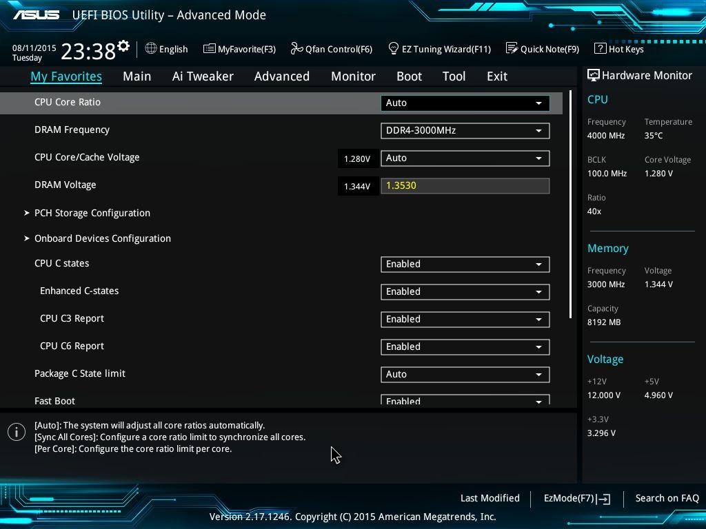
Pressing F7 opens the traditional UEFI or advanced options. The main tabs have remained the same. Let’s look at them one by one.
My Favorites : This is for quick access of the most used settings without searching for them in the heaps of things available.
Main : Presents essential information about the BIOS, Processor, Memory, System Time/Date/Language. Also has the option to set administrator passwords for the UEFI.
Ai Tweaker: This is the main page for tweaking and overclocking the processor and memory. With Skylake, we see the advent of newer options like BCLK-DRAM frequency ratio. This being a mainstream board (read non-ROG) the options available are still not borderline crazy, but there are enough things for a seasoned overclocker to play with.
An interesting option here is the option to select CPU SVID support, which when enabled opens the route for the CPU to communicate with the external voltage regulator.
Advanced: Contains settings related to CPU (Power), System Agent, Network Stack, USB, PCH, Onboard Devices etc.
A new addition here is Intel Thunderbolt related options. Thunderbolt is enabled by the Alpine Ridge controller from Intel, and here we can see the specification versions as well as options to boot from a Thunderbolt device.
In Platform configuration there are options to select DMI Link settings. The maximum link speed can also be selected from here.
USB configuration contains settings for newer supported technologies such as XHCI. Settings for USB Type C can also be found in the Advanced section.
You also get information about SMART supported hard disc drives.
Monitor: Temperature/Voltage/Fan speeds can be monitored from here. ASUS has added Water Pump Speed/Control in this menu.
Boot: Regular boot sequence/override options.
Tools: There are a couple of UEFI tools that ASUS provide with the Z170-A.
ASUS Overclocking Profile lets users save a custom profile which can then be accessed later to load the values.
Software walkthrough:
ASUS’ software implementation has always been centred on their AI Suite utility, a central hub for their other programs/software to function. I ran into some issues with the Z170-A where I couldn’t install AI Suite 3, so I thought to cover other software that came aboard. I will be covering AI Suite for Skylake in a future review.
The installer has received the same paintjob as that of the UEFI. ASUS splits the bundle into drivers, utilities and then added software bonuses. Added third-party software include Daemon Tools Pro, an imaging software, WinZip, Chrome Browser and Norton Security.
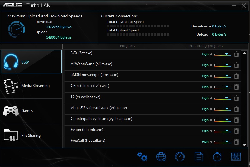
Turbo LAN is ASUS’ custom network prioritizing and monitoring software built on top of cFOS LAN.
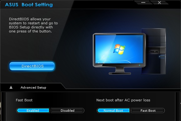
ASUS Boot Setting provides an option to directly boot into BIOS without pressing a button. There are also options for fast boot and wake after sudden power loss.
Test Setup:
The following test system was used for this review:
- Intel Core i7-6700K, 4C/8T, Skylake, 4GHz base, 4.2GHz turbo
- ASUS Z170-A motherboard, BIOS 0404
- G.SKILL Ripjaws4 DDR4-3000 memory, 8GB, 15-15-15-35-2T
- ASUS R9 290X Matrix GPU, Hawaii
- Kingston SSDNow V300 64GB SSD for boot drive and benchmarks
- Corsair AX760i 80Plus Platinum Power Supply
- Corsair H100i AIO Closed loop CPU cooler
- Open Test Bench
Benchmarks:
I compared the i7-6700K with the earlier motherboards I had reviewed. I also took two of my friends’ help to get some data about the i7-2600K and i7-4790K. A keen eye can easily observe that not all benchmark numbers were collected for these two processors, but in most of the benchmarks I have tried to include them to see the performance difference between two generations.
Let’s fire up our usual suite of benchmarks first.
3D Particle Movement is a benchmark penned by Dr.Ian Cutress (Lead Reviewer, AnandTech) and it works by taking basic 3D movement algorithms used in Brownian Motion simulations and testing them for speed. High floating point performance, MHz and IPC wins in the single thread version, whereas the multithread version has to handle the threads and loves more cores.
Next up is Cinebench in its three most popular variants. Cinebench is a popular rendering program.
I started to include Web based benchmarks quite some time back in my review. While most of them utilize JavaScript, they run a variety of tests which can stress your system quite hard.
Kraken is Mozilla’s well-known benchmark that measures the speed of several different test cases extracted from real-world applications and libraries. The overall layout is built on SunSpider, another popular JavaScript based benchmark.
As for the overclocking, I took two routes to see how the chip and the board fared. The first amongst them was simple multiplier based overclocking where I didn’t touch BCLK settings and played with VCore and multipliers. The second was purely on BCLK based settings.
For the i7-6700K, the maximum overclock achieved through multipliers was 4.8GHz at 1.35v VCore with 100MHz BCLK and 48x multiplier.
For the i7-6700K, the maximum overclock achieved through multipliers was 4.6GHz at 1.35v VCore with 200MHz BCLK and 23x multiplier.
Conclusion:
I think Skylake demands a conclusion of its own. In this review, we have covered its flagship desktop part, the Core i7-6700K. With desktop Broadwell as elusive as the Bigfoot, our best chance to analyse performance of Intel’s 14nm parts. Intel had a couple of things to consider when it moved to its next generation of processors. Firstly, per-generation performance yield was in single digit percentages. Secondly, with each new generation the general overclocking potential for a consumer-grade chip went down by a notch. Lastly, since Ivy Bridge, Intel processors have been plagued with thermal issues, and a majority of it hovered around Intel’s choice of TIM. While I cannot conclude about Skylake’s other representatives, the Core i7-6700K, performance wise, is a mixed bag. In some tests it bests Intel’s 4790K by quite some margin, and in some it loses to it. It wins more than it loses, however. When compared to even older i7-2600K, the performance gap is larger across the board. In some tests the performance increase is 50%. People with Sandy Bridge systems will definitely see a nice boost in overall performance. For Haswell and above, the upgrade may not be worth it if you are only considering raw CPU performance.
But the real gem is the Z170 chipset itself. Intel has introduced a lot of new features with its Alpine Ridge controller, providing 26 PCIe lanes via its HSIO plus USB3.1 Gen2, Thunderbolt and DisplayPort to name a few. That means no PCIe bandwidth issues – M.2 and SATA Express can be used at once. Updated DMI means faster interconnect between CPU and PCH, and Intel’s RST upgrades mean three plus PCIe storage devices can be used in RAID. Intel’s Jacksonville network controller debuts with Z170 as well; in essence significantly upping the ante for Skylake based systems.
Let’s look at the motherboard then. ASUS’ Z170-A represents their (arguably) lowest end of the mainstream range, but the feature sets provided with this board left me baffled about its pricing. The Z170-A will be retailing for Rs.14775 (Plus taxes). While this is lower than what I expected, the entire sub-20K INR range is a segment fiercely contested by other brands. It may also come into direct competition with its ROG brethren. Aesthetic wise, this is a clear departure from ASUS’ Z97 boards and more in line with their X99 setup. Feature wise, you get a ten phase fully digital VRM, onboard Power and XMP switches, six SATA 6Gbps ports, a full x4 M.2 slot, three PCIe x16 slots (though the last one is wired x4), bunch of USB3.0 internal headers and external ports, two USB3.1 Gen2 ports in both flavours (Type-A and Type-C) via the AsMedia controller and EMI shielded audio courtesy of Crystal Sound 3. Adding to the mix ASUS’ upgraded UEFI that offers more features in a mainstream board like the Z170-A and their fully decked out software bundle, the entire package is very lucrative. The overclocking performance was pleasantly surprising as well, with my i7 sample reaching 4.8GHz with an AIO liquid cooler. My only gripes are the lack of an on-board LED debug display and any wireless connectivity. But then I may be asking for too much. With good looks and performance to match, ASUS’ Z170-A might be the first strike that the company needs. Whether it can reign supreme will be seen shortly.
The Z170-A deserves a gold award for its performance, aesthetics and the complete bundle it provides. With the new chipset, ASUS has stuck with what worked best for them and then matured the ecosystem of UEFI and software. The upgraded hardware has made its way into the first member of the mainstream league, bringing along good performance across the board. When you consider the price, it looks even more value for money. For Skylake, my complete conclusion will be out once I test the Core-i5 variant as well, but for now, if you are using Haswell/Devil’s Canyon, the only reason you should choose Intel’s 14nm processor is for the chipset itself. And oh, if you love BCLK based overclocking, that is.
