
BIKeINSTEIN
Herald
Read it at the below link. There's more in the subsequent posts-
https://forums.anandtech.com/threads/ryzen-strictly-technical.2500572/
Copy-pasted only the original post content below; there's more in the subsequent posts at the source.
(Also there could be errors or something missing.)
P.S.
Dear Mods,
Please move/delete or whatever as you may find it appropriate if repost or flouting any rules. This deserved it's own thread IMHO.")
https://forums.anandtech.com/threads/ryzen-strictly-technical.2500572/
Copy-pasted only the original post content below; there's more in the subsequent posts at the source.
(Also there could be errors or something missing.)
This is by no means a full blown review. It just provides some of the more in-depth information, along with some test results.
- CCX - Compute Complex. Consists of four Zen cores and a shared 8MB L3 cache.
- PState - Performance State. Specifies the CPU multiplier and voltage when residing in the state.
- Zeppelin – Codename of the die design used in Summit Ridge (AM4), Snowy Owl (SP4) and Naples (SP3) Zen based CPUs.
- dLDO – Digital low-dropout voltage regulator.
- XFR – Extended Frequency Range
- MACF - Maximum all core frequency.
- MSCF – Maximum single core frequency.
- ACXFRC – All core XFR ceiling
- SCXFRC – Single core XFR ceiling
- SMU – System management unit.
SMU – The master of puppets
Due to the seamless integration of the on-die system management unit (SMU, similar in functionality to PMU on Intel) there are quite many differences compared to the previous AMD desktop microarchitectures when it comes to overclocking.
At stock, Ryzen has all of the power management features enabled and the SMU runs the whole operation and is in charge for everything. These power management features include various power, current and thermal limiters, voltage controllers and power gating features.
All of these can be completely ignored, if you have no plans to overclock the CPU.
For overclocking purposes the engineers at AMD have included a special mode (the "OC Mode"), which will disable all of the limiters, voltage controllers and protections (except the CPU thermal protection) upon the activation.
The "OC Mode" is automatically activated when the user raises the base frequency (P0 PState) of the CPU. The SMU indicates the activation of the "OC Mode" by sending "0C" code to the diagnostic display (Port 80) of the motherboard.
Understanding the different CPU frequency states (PStates), their voltages and especially the actual effective voltage is harder than ever before with Zeppelin. Unlike with the older designs (15h family) the boosted PStates (Turbo & XFR) are completely invisible.
Due to that fact, they are officially called as "Shadow PStates". This means that unlike with the previous designs these PStates are not defined in the standard MSR registers and cannot be modified (or be seen) by the user. The only way the user can even verify their presence is to see them actually firing (i.e. from the actual effective frequency & voltage).
Understanding the voltages specified for the standard PStates can be confusing as well. That's because in the normal operating mode (i.e. "non-OC") the SMU controls the voltages automatically through the voltage controllers.
For example, the P0 PState might specify 1.37500V voltage, while the actual effective voltage during the residency in this state is 1.26250V or slightly higher. This is not a glitch, but the normal operation of the CPU. Basically, the voltage specified in the MSR is just the upper limit and the SMU will automatically add a dynamic negative offset to this value, reducing the actual effective voltage. The amount of the negative offset varies depending on load and the temperature. For the tested sample the offsets were -120mV & -144mV for the two highest base PStates (3.6 & 3.2GHz).
When the "OC Mode" is activated the SMU will disable the voltage controllers, which among other things disables the automatic voltage offsets. This can create an illusion that the power consumption is heavily increasing due to the use of "OC Mode". While technically it is accurate, it is more of a consequence than the actual reason. A vast majority of the increased power consumption comes from the now disabled automatic negative voltage offsets, which causes the actual CPU voltage to increase anything between 50 and 150mV. Because of this behavior, it is advised that the user doesn't increase the CPU voltage right away (when overclocking), but only upon actual demand (as usual).
One of the major down sides of the "OC-Mode" is that upon activation both Turbo and XFR will be disabled as well. Basically, this means that unless you are able to reach at least the default MSCF / XFR frequency on all cores, then you will essentially be losing single threaded performance compared to stock configuration.
The XFR
The XFR (Extended Frequency Range) is essentially an extension or enhancement to the standard CPB (Turbo) algorithm. In scenarios where all of the various limiters (power, current and thermal) have margins, the CPU is allowed to boost above its nominal base and boost speeds. Just like the standard CPB algorithm, the XFR has separate clock ceilings for a single core and all core operation.
For example, for the 1800X SKU the clock configuration is following: 3.6GHz all core frequency (MACF), 4.0GHz single core frequency (MSCF), 3.7GHz maximum all core XFR ceiling (ACXFRC) and 4.1GHz maximum single core XFR ceiling (SCXFRC).
The number of XFR bins (n x 100MHz) might vary between the different SKUs, however for the 1800X model there is a single XFR bin available for both all core and single core operations. In typical consumer workloads, the CPU will generally be able to reside in the XFR states (3.7GHz / 4.1GHz) constantly, however in certain specialized workloads (such as Linpack or Prime95) the frequency usually decreases towards the base frequencies (3.6GHz / 4.0GHz).
The base-clock (BCLK)
Overclocking the base clock (BCLK) on AM4 platform is possible, however generally not recommended. This is due to its frequency relations with other interfaces, such as the PCIe. Unlike with Intel's more recent CPUs, there is no asynchronous mode (straps / gears) available, which would allow stepping down the PCIe frequency at certain intervals. The PCIe frequency relation is fixed and therefore it increases at the same rate with the BCLK. Gen. 3 operation can generally be sustained up to ~107MHz frequency and higher speeds will usually require forcing the links to either Gen. 2 or to Gen. 1 modes.
Unstable PCIe can cause various issues, such as system crashes, data corruption (M.2 SSDs), graphical artifacts and various kinds of other undefined behavior.
The internal voltage regulation (dLDO)
Zeppelin is the first design in which AMD has extensively utilized integrated voltage regulators. Unlike the fully integrated voltage regulator (FIVR) used in Haswell and Broadwell CPUs, AMD's regulator implementation isn't based on ultra-high speed switching circuitry. The integrated voltage regulators in Zeppelin are ultra-high efficiency digital low-dropout (dLDO) type of regulators. Most of the different domains (cores, caches, data fabric, etc.) have their own dLDOs and they can all be controlled individually.
Despite the presence of the dLDOs, the consumers can ignore them completely. This is because in the consumer parts most of the dLDOs (all except some of the minor domains) are permanently placed in a by-pass mode. This means that actual regulators are disabled and all of the voltage regulation takes place on the motherboard, just like on the previous generation CPUs and APUs.
The frequency relations of the CCX
In terms of the internal die frequency relations, Zeppelin is quite different to the previous designs. The core, L1 and L2 cache speed is permanently linked together as usual, however unlike with the previous designs the L3 cache now operates at core speed as well (i.e. full speed). Since the L3 cache is shared between the cores within the same CCX, the L3 frequency is synchronized with the currently highest clocked core of the CCX it belongs to. In normal conditions, all of the cores within a CCX operate at the same speed, or alternatively are power gated.
The structure of the CCX sets few rules that one should know prior starting changing the settings from stock. Each of the four cores within a CCX must be running at the same frequency (i.e. reside in the same PState) or be power gated. While this is the official truth, the rule doesn't fully apply in practice. It is entirely possible to command the individual cores within the same CCX to different PStates, however the results in many cases are not what was originally expected. This is due to the internal frequency relations of the CCXs.
While each of the cores and their full speed L1 & L2 caches can be clocked independently, the shared L3 cache frequency is linked to the currently highest clocked core speed within the CCX at all times. Because of that there will be frequency difference dependent delta between the requested and the actual frequency, if all of the cores within the CCX don't have a common frequency.
The effective CPU multiplier consists of two components: CPUFID and CPUDFSId. The CPUFID is an integer value ranging from 16 to 255. The CPUDFSId is a floating-point value between 1 and 6. Due to the natural divider of 8 for the CPUDFSId, its adjustment step is always 0.125 (1/8). The effective multiplier is produced with following formula: ((CPUFID / (CPUDFSId / 8)) / 4).
In cases where the cores within a CCX a clocked differently, calculating the effective multiplier is somewhat more complex. If all of the different PStates have the same CPUDFSId value, the effective multiplier can be calculated with following formula: Target core CPUFID / (1 + ((highest core CPUFID - target core CPUFID) / highest core CPUFID)). For example, if the highest core multiplier is 36.0x (CPUFID = 144 & CPUDFSId = 1) and the target multiplier for other cores is 32.0x (CPUFID = 128 & CPUDFSId = 1): 128 / (1 + ((144 - 128) / 144)) = 115.2 (28.8x). Further rules and limitations may apply, depending on the used CPUDFSId values and the actual frequency.
The synchronization of the data fabric dictates that each of the enabled CCXs have identical number of cores enabled at all times. The available configurations are 1 (1:0), 2 (2:0 or 1:1), 3 (3:0), 4 (4:0 or 2:2), 6 (3:3), 8 (4:4).
The data fabric
The northbridge of Zeppelin is officially called as the data fabric (DF). The DF frequency is always linked to the operating frequency of the memory controller with a ratio of 1:2 (e.g. DDR4-2667 MEMCLK = 1333MHz DFICLK). This means that the memory speed will directly affect the data fabric performance as well. In some cases, it may appear that the performance of Zeppelin scales extremely well with the increased memory speed, however that is necessarily not the case.
In many of these cases the abnormally good scaling is caused by the higher data fabric clock (DFICLK) resulting from the higher memory speed, rather than the increased performance of the memory itself.
The highest officially supported memory speed for consumer (AM4) Zeppelin parts is 2667MHz (two single rank / sided modules in total) or 2400MHz (two dual rank / sided modules in total), however memory ratios for 2933MHz and 3200MHz speeds are available (not officially supported), at least on some motherboards.
Overclocking
The overclocking headroom for the higher-end Ryzen models is rather slim. This was expected due to the relatively high stock frequencies, high-density orientation of the design and the low power targeted manufacturing process used for the Zeppelin die (Samsung 14nm LPP).
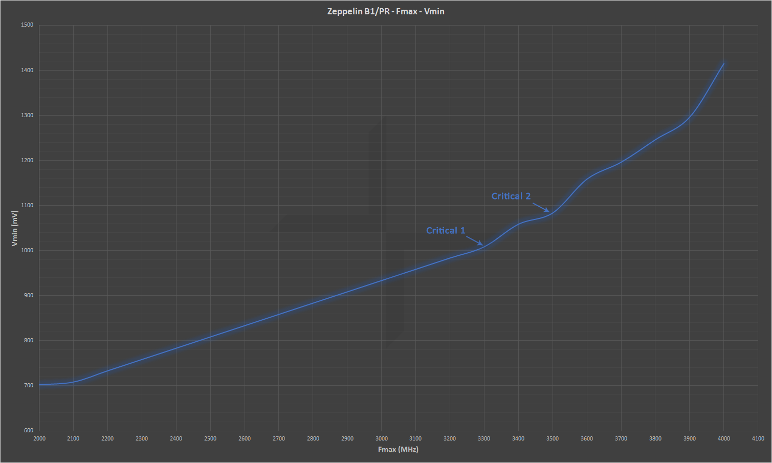
As indicated by the Vmin-Fmax curve, Zeppelin's voltage scaling is perfectly linear until 3.3GHz (25mV per 100MHz). The first deviation ("Critical 1") from this linear behavior can be seen at 3.3GHz. The second and the final deviation ("Critical 2") can be seen at 3.5GHz. Beyond this point the voltage scaling is neither linear or recovers even temporarily, and the CPU is requiring higher voltage in increasingly larger steps to scale further.
The ideal frequency range for the process or the design (as a whole) appears to be 2.1 - 3.3GHz (25mV per 100MHz). Above this region (>= 3.3GHz) the voltage scaling gradually deteriorates to 40 - 100mV+ per 100MHz.
This means that at ~3.8GHz pushing further usually becomes extremely costly (power / thermal wise).
In comparison, the "critical" points for the two previous AMD desktop designs were at:
- Orochi Rev. C aka Vishera, 32nm SHP SOI - (1 = 4.4GHz, 2 = 4.7GHz)
- Kaveri / Godavari, 28nm "SHP" HPP Planar - (1 = 4.3GHz, 2 = 4.5GHz)
The voltage scaling indicated by the Vmin-Fmax curve (above) can be also clearly seen in the default voltages for the different frequency states (PStates) of the CPU.
On the high-end models the actual (effective) voltage for the base frequency (e.g. 3.6GHz on 1800X SKU) can be anything between 1.200 - 1.300V. Meanwhile the actual (effective) voltage for the highest single core boosted PState (XFR, e.g. 4.1GHz) can be as high as 1.47500V.
In the tested sample the actual default voltage for the base frequency (P0, 3.6GHz) was ~1.25000V, while the highest single core boost state (XFR, 4.1GHz) defaulted to 1.4625V.
While AMD has not revealed the highest safe (sustainable) VDDCR_CPU (CCX) or VDDCR_SOC (data fabric & peripheral) voltage levels, it can be speculated that voltages higher than 1.4500V are generally not advisable for sustained use, at least in conditions / workloads which result in high power consumption (i.e. all cores fully stressed).
Despite it is true that the high-end models can have their default voltage set up to 1.47500V during their maximum single core boost (XFR) operation, the power consumption / dissipation, amount of current flowing and the temperatures are very different between the scenarios where only a single core is fully stressed or all of the cores are fully stressed.
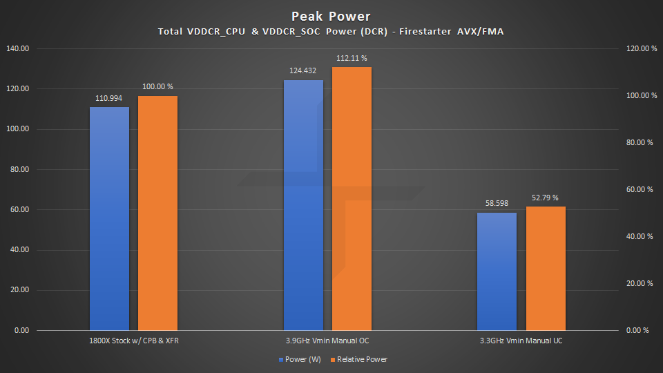
Pushing to or even beyond the factory MSCF (4.1GHz / XFR) frequency is entirely possible on all cores, however in my personal opinion it is not worth the significantly higher power consumption resulting from the significantly increased supply voltage. Personally, if find it more intriguing to try making the CPU even more efficient than it already is at stock.
Overclocking Ryzen, at least the higher-end models is kind of a double-edged sword. Due to how the Turbo / XFR operates in Zeppelin and the rather slim overclocking margins, the user might end up actually losing single core performance when the CPU is overclocked. Since the Turbo / XFR will always be disabled when the CPU is overclocked (upon entering the “OC-Mode”), the single core performance might actually be lower than at stock, if the user is unable to reach the same speed on all cores as the CPU operated at single core stress at default (e.g. 4.1GHz on 1800X SKU).
The power consumption
All of the power consumption measurements have been made with DCR method. The figures represent the total combined power consumed by the CPU cores (VDDCR_CPU, Plane 1) and the data fabric / the peripherals (VDDCR_SOC, Plane 2). These figures do not include switching or conduction losses.
Peak power (i.e. worst-case) figures were measured during Firestarter FMA/AVX binary execution. On average the resulting power consumption is around 30% higher than the power consumption resulting from any other real world consumer, fully multithreaded workload.
Note: Current versions of Prime95 (28.10) do not stress Ryzen CPUs properly. The resulting power consumption is abnormally low, and both Firestarter and Linpack result in significantly higher power consumption.
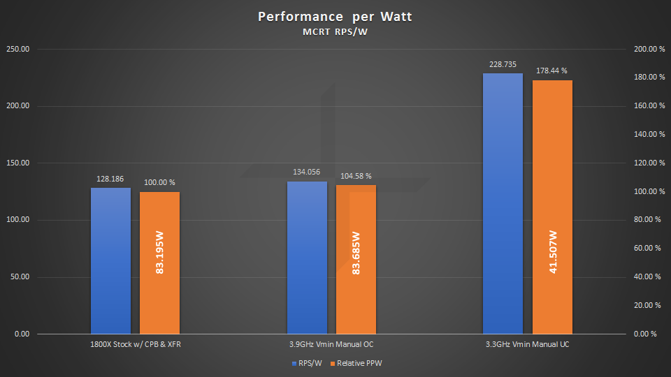
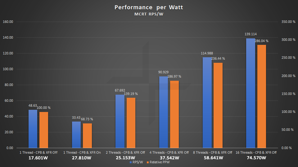
"MCRT" (Monte Carlo raytracer, based on SmallPT) was chosen as a more real world representative workload. It provides extremely good and linear multithreaded scaling and is a relatively modern workload.
Rather than just measuring the average power consumption, performance per watt metric was included as well to provide an additional data point.
An easter egg
Zeppelin features a highly advanced power management, as stated many times before. Just like Carrizo / Bristol Ridge, which feature a very similar PM, Zeppelin can infact support cTDP as well. cTDP is not officially supported (or available) on any consumer Zeppelin based SKU (AFAIK). The lack of official support is merely a distraction
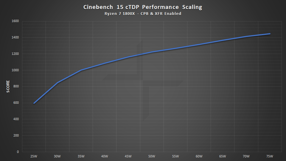
850 points in Cinebench 15 at 30W is quite telling. Or not telling, but absolutely massive. Zeppelin can reach absolutely monstrous and unseen levels of efficiency, as long as it operates within its ideal frequency range.
In case you have "any" questions, just ask.
EDIT: 3/6/2017
Ok, so I've now changed the charts to have a common Y-axises, where possible.
An additional data point was added to the charts to indicate performance with 256-bit workloads excluded (the ones which have actual gains from 256-bit code).
The excluded 256-bit workloads are: Blender, Bullet (IPC only), Embree, Euler3D, Himeno, Linpack, NBody & X265.
I also noticed that there is an error, affecting Kaby Lake results in 4C/4T, 4C/8T and SKU vs. SKU tests. The absolute data is correct, however the summary views are affected by a tiny amount.
This is because I made a typo in "Caselab Euler3D" calculation for Kaby Lake (reversed calculation). Because of that the summary views will show small changes for Kaby Lake only. In 4C/4T summary the difference will reduce by >= 0.5% and in 4C/8T increase by ~1% (same applies to SKU vs. SKU).
I leave the gallery codes (Imgur) to the original charts in the OP after changing the charts, so anyone can inspect the results if necessary.
")
P.S.
Dear Mods,
Please move/delete or whatever as you may find it appropriate if repost or flouting any rules. This deserved it's own thread IMHO.
