DIY Printed Circuit board Making.
Printed circuit board or PCB has its vital role in today’s high-tech life. From TV to toys from Computer to mobile, all electrons work with a PCB inside. Commonly a PCB is made up of a fiber board with copper tracks to join different electronic components together so that they can acts as a single unit or circuit. A PCB can have from a single layer of copper connection used in common electronics like toys, in pc mouse etc, or can have up to seven connection layers in single PCB used in Computer motherboard or mobile phone PCB.
Today by this small tutorial I like to share with you the most common process of DIY PCB making at your home. I came to know this process in my school time, but one can Google and find many process of PCB making. Secondly I adopted this process because it’s very easy and low in resources. There is no proper name for this process but generally it’s called “Laser print PCB etchingâ€.
As the name says a laser printout is etched on a blank PCB.
Items needed:
1. PC and a Laser Printer (to design and printout the circuit layout).
2. Toner Transfer Paper (to transfer the toner layout on to the PCB).
3. Blank PCB.
4. Hex blade, zero no. sandpaper and files (to cut the desire piece of PCB, polish and file the rough surface).
5. Lamination Machine.
6. Ferric Chloride and Iso-Propanol.
7. Plastic washing tray and brushes.
8. Drill bits to drill holes on to the PCB for component placement.
Few WARNIGS:-
1. Be very care full when using cutting or drilling tools. If you are not familiar with these tools better get help from a professional.
2. Be very-very careful when working with CHEMICALS. Try not to come in direct contact with the chemical, if so immediately wash the effected body part with lot of running water.
3. For eching process FeCl3 solution is needed. When adding H20 to FeCl3, fumes of HCL is releases which is harmful when inhaled.
Now let’s get started. In this tutorial I am making a 4-channel Fan Controller.
Initial circuit design and layout is done.


Now printing the layout on to the toner transfer paper.

Now cutting the blank PCB.


Now use sand paper to make the PCB clean and shiny.

Role the PCB and printout through the lamination machine, this will stick the paper onto the PCB. Now leave the PCB in soap water for an hour and then genteelly peel off the paper. Now PCB has only toner in the form of the circuit layout.


Now it’s time to bring the chemicals in action.

Add some distilled water in a plastic tray. (USE ONLY CHEMICAL DISTILLED WATER) battery water has some acid properly.

Now add FeCl3 powder.

Hot exothermic reaction, HCL fumes are librated.

Drop the PCB in.

Leave it for an Hour.


Look carefully Fecl3 is eating the copper.


After etching only toner is left.

Clean the PCB with Iso-Propanol.


This removes the toner and shiny copper tracks are left.


it’s time to drill some holes. I am using 1mm drill bit and a DC motor for this job.


Done. Your PCB is now ready to be fitted with the components.


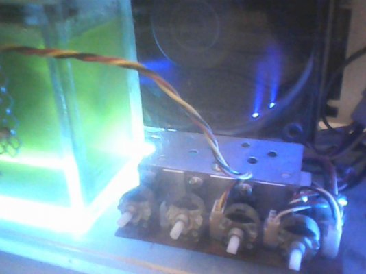
All assembled and undergo testing. Seems everything is fine and the circuit is working perfectly.

Some pics of final product.


This finishes my tutorial. Hope you like it.
I have tried my best to put this tutorial in good shape, but still please ignore any mistakes.
Thanking
Rakesh Sharma
Printed circuit board or PCB has its vital role in today’s high-tech life. From TV to toys from Computer to mobile, all electrons work with a PCB inside. Commonly a PCB is made up of a fiber board with copper tracks to join different electronic components together so that they can acts as a single unit or circuit. A PCB can have from a single layer of copper connection used in common electronics like toys, in pc mouse etc, or can have up to seven connection layers in single PCB used in Computer motherboard or mobile phone PCB.
Today by this small tutorial I like to share with you the most common process of DIY PCB making at your home. I came to know this process in my school time, but one can Google and find many process of PCB making. Secondly I adopted this process because it’s very easy and low in resources. There is no proper name for this process but generally it’s called “Laser print PCB etchingâ€.
As the name says a laser printout is etched on a blank PCB.
Items needed:
1. PC and a Laser Printer (to design and printout the circuit layout).
2. Toner Transfer Paper (to transfer the toner layout on to the PCB).
3. Blank PCB.
4. Hex blade, zero no. sandpaper and files (to cut the desire piece of PCB, polish and file the rough surface).
5. Lamination Machine.
6. Ferric Chloride and Iso-Propanol.
7. Plastic washing tray and brushes.
8. Drill bits to drill holes on to the PCB for component placement.
Few WARNIGS:-
1. Be very care full when using cutting or drilling tools. If you are not familiar with these tools better get help from a professional.
2. Be very-very careful when working with CHEMICALS. Try not to come in direct contact with the chemical, if so immediately wash the effected body part with lot of running water.
3. For eching process FeCl3 solution is needed. When adding H20 to FeCl3, fumes of HCL is releases which is harmful when inhaled.
Now let’s get started. In this tutorial I am making a 4-channel Fan Controller.
Initial circuit design and layout is done.


Now printing the layout on to the toner transfer paper.

Now cutting the blank PCB.


Now use sand paper to make the PCB clean and shiny.

Role the PCB and printout through the lamination machine, this will stick the paper onto the PCB. Now leave the PCB in soap water for an hour and then genteelly peel off the paper. Now PCB has only toner in the form of the circuit layout.


Now it’s time to bring the chemicals in action.

Add some distilled water in a plastic tray. (USE ONLY CHEMICAL DISTILLED WATER) battery water has some acid properly.

Now add FeCl3 powder.

Hot exothermic reaction, HCL fumes are librated.

Drop the PCB in.

Leave it for an Hour.


Look carefully Fecl3 is eating the copper.


After etching only toner is left.

Clean the PCB with Iso-Propanol.


This removes the toner and shiny copper tracks are left.


it’s time to drill some holes. I am using 1mm drill bit and a DC motor for this job.


Done. Your PCB is now ready to be fitted with the components.


All assembled and undergo testing. Seems everything is fine and the circuit is working perfectly.

Some pics of final product.


This finishes my tutorial. Hope you like it.
I have tried my best to put this tutorial in good shape, but still please ignore any mistakes.
Thanking
Rakesh Sharma


