
My E4300 Overclock Results
- Thread starter nj_gamer
- Start date
You are using an out of date browser. It may not display this or other websites correctly.
You should upgrade or use an alternative browser.
You should upgrade or use an alternative browser.
- Status
- Not open for further replies.
Memory timings
Memory performance is not entirely determined by bandwidth or MHz, but also the speeds at which it responds to a command or the times it must wait before it can start or finish the processes of reading or writing data. These are memory latencies or reaction times (timings). Memory timings control the way your memory is accessed and can be either a contributing factor to better or worse 'real-world' performance of your system.
Internally DRAM has a huge array of cells that contain data. (If you've ever used Microsoft's Excel, try and picture it that way) A pair of row and column addresses can uniquely address each cell in the DRAM. DRAM communicates with a memory controller through two main groups of signals: Control-Address signals and Data signals. These signals are sent to the RAM in order for it to read/write data, address and control. The address is of course where the data is located on the memory banks, and the control signals are various commands needed to read or write. There are delays before a control signal can be executed or finish and this is where we get memory timings.
The standard format for memory timings are most often expressed as a string of four numbers, separated by dashes, from left to right or vice-versa like this 2-2-2-5 [CAS-tRCD-tRP-tRAS] . These values represent how many clock cycles long each delay is but are not expressed in the order in which they occur. Different bioses will display them differently and there maybe additional options (timings) available.
Which timings mean what?
In most motherboards, numerous settings can be found to optimize your memory. These settings are often found the Advanced Chipset section of the popular award bioses. In certain instances, the settings maybe placed in odd locations and even given unfamiliar names, so please consult your motherboard manual for specific information. Below are common latency options:
* Command rate - is the delay (in clock cycles) between when chip select is asserted (i.e. the RAM is selected) and commands (i.e. Activate Row) can be issued to the RAM. Typical values are 1T (one clock cycle) and 2T (two clock cycles).
* CAS (Column Address Strobe or Column Address Select) - is the number of clock cycles (or Ticks, denoted with T) between the issuance of the READ command and when the data arrives at the data bus. Memory can be visualized as a table of cell locations and the CAS delay is invoked every time the column changes, which is more often than row changing.
* tRP (RAS Precharge Delay) - is the speed or length of time that it takes DRAM to terminate one row access and start another. In simpler terms, it means switching memory banks.
* tRCD (RAS (Row Access Strobe) to CAS delay) - As it says it's the time between RAS and CAS access, ie. the delay between when a memory bank is activated to when a read/write command is sent to that bank. Picture an Excel spreadsheet with a number across the top and along the left side. They numbers down the left side represent the Rows and the numbers across the top represent the Columns. The time it would take you, for example, to move down to Row 20 and across to Column 20 is RAS to CAS.
* tRAS (Active to Precharge or Active Precharge Delay) - controls the length of the delay between the activation and precharge commands ---- basically how long after activation can the access cycle be started again. This influences row activation time which is taken into account when memory has hit the last column in a specific row, or when an entirely different memory location is requested.
These timings or delays occur in a particular order. When a Row of memory is activated to be read by the memory controller, there is a delay before the data on that Row is ready to be accessed, this is known as tRCD (RAS to CAS, or Row Address Strobe to Column Access Strobe delay). Once the contents of the row have been activated, a read command is sent, again by the memory controller, and the delay before it starts actually reading is the CAS (Column Access Strobe) latency. When reading is complete, the Row of data must be de-activated, which requires another delay, known as tRP (RAS Precharge), before another Row can be activated. The final value is tRAS, which occurs whenever the controller has to address different rows in a RAM chip. Once a row is activated, it cannot be de-activated until the delay of tRAS is over.
The Memory FAQ - PC Perspective Forums
Read this article for more info regarding RAM..
hope this helps
")
@baasha
Thanks for the info
Now OCCT is stable after running it for 2 hrs..Ram could not be overclocked ,kept giving errors.So ran it at default speed and voltage so its stable now.
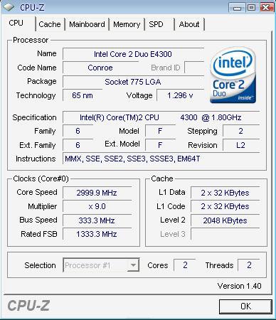
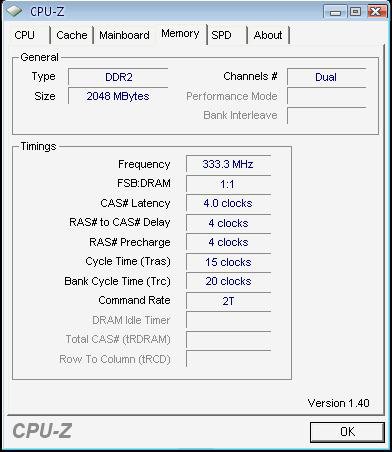
Final overclock:
FSB-1333MHz
DRAM:666.4MHz
FSB: DRAM:1:1
timings 5-5-5-15 at 2T
So what do i do to reduce the timings? i first reduced it to 4-4-4-15,Gave errors..So do i tinker with the volts?
Thanks for the info
Now OCCT is stable after running it for 2 hrs..Ram could not be overclocked
,kept giving errors.So ran it at default speed and voltage so its stable now.Final overclock:
FSB-1333MHz
DRAM:666.4MHz
FSB: DRAM:1:1
timings 5-5-5-15 at 2T
So what do i do to reduce the timings? i first reduced it to 4-4-4-15,Gave errors..So do i tinker with the volts?
Keep the memory timings at default, first switch to 1T, I think this makes more of an impact...do so at 2.0V
If that gives an error switch back to 2T and 4-4-4-15 at 2.0V
Oh and you are running RAM unlinked na, cause IIRC to successfully OC the RAM on this chipset the RAM should be unlinked.
If that gives an error switch back to 2T and 4-4-4-15 at 2.0V
Oh and you are running RAM unlinked na, cause IIRC to successfully OC the RAM on this chipset the RAM should be unlinked.
use coretemp for temperatures..
between speedfan and everest stick to speedfan..
if u wanna check if tweaking ur overclocks/mem timings is actually yeilding any performance gains, then use SuperPI..that way u can see wats suits ur system best, as far as speed is concerned..
heres the link:
Super PI Mod 1.5
between speedfan and everest stick to speedfan..
if u wanna check if tweaking ur overclocks/mem timings is actually yeilding any performance gains, then use SuperPI..that way u can see wats suits ur system best, as far as speed is concerned..
heres the link:
Super PI Mod 1.5
Ran memtest for 6 passes(took 3hrs 20min)No errors detected.Playing with Super Pi now(thanks baasha).Man overclocking is fun as well as boring(since u have to run the stress test for 2 hrs worrying whether the proccy will burn out and another 3hrs for memtest).
So shall i leave the overclock for now or tweak it somemore?Say try to push it to 4-4-4-12 16?
So shall i leave the overclock for now or tweak it somemore?Say try to push it to 4-4-4-12 16?
about overclocking/tweaking ur RAM..
Best option is to read around in different forums and see how far people have been able to go this far with this RAM..a lot of people on TE have this RAM..u cud ask them..i'm sure they wud help..
Now that u r stable at 4-4-4-15 2T all auto, try the following:
1. Try bumping up the RAM clocks in small 15-20 Mhz increments, and boot up..run orthos for a while and make sure everything is stable. then as come closer to 800 Mhz, lets say 770-780 Mhz, run orthos for longer..run memtest as well if u can..do this until u have found the maximum stable value...
run SuperPI and see wat results u get against the RAM at default value..
2. Now that u have achieved the maximum clock ur RAM can do, try the tightening the timings..
do this by starting up from all settings at default..!!
set the timings to 4-4-4-12 2T and run orthos for some time and also superPI..record ur results..
now overclock ur RAM and see when the RAM becomes unstable...
find out the maximum stable settings for these timings, i.e. 4-4-4-12 2T..
check ur SUPER PI scores and decide wat settings u wanna keep...
phew..!! hope this helps...
overclocking is not an easy job..it requires a lot patience and time..but it pays off very well in the end

- Status
- Not open for further replies.